


Chapter 4 Connecting Signals
NI 6115/6120 User Manual 4-18 ni.com
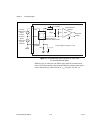
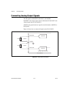
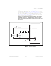
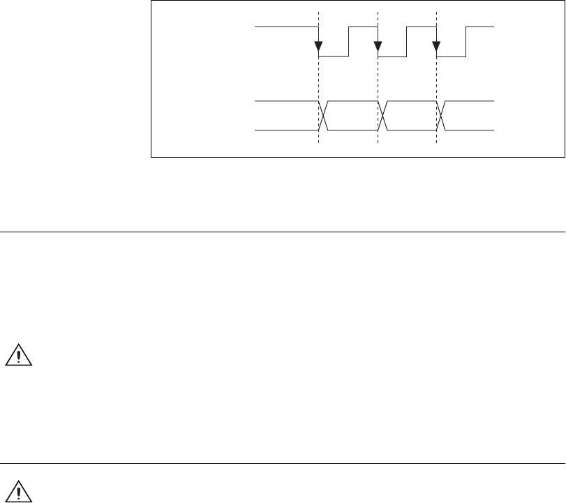
Figure 4-10 shows a DIO operation driven by an RTSI clock signal on its
falling edge.
Figure 4-10. Falling-Edge RTSI Clock Signal Driving a DIO Signal
Power Connections
Two pins on the I/O connector supply +5 V from the computer power
supply using a self-resetting fuse. The fuse resets automatically within a
few seconds after the overcurrent condition is removed. These pins are
referenced to DGND and can be used to power external digital circuitry.
The power rating is +4.65 to +5.25 VDC at 1 A.
Caution Under no circumstances should you connect these +5 V power pins directly to
analog or digital ground or to any other voltage source on the NI 6115/6120 or any other
device. Doing so can damage the NI 6115/6120 and the computer. NI is not liable for
damage resulting from such connections.
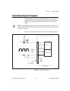
Connecting Timing Signals
Caution Exceeding the maximum input voltage ratings, which are listed in Table 4-3, can
damage the NI 6115/6120 and the computer. NI is not liable for any damage resulting from
such signal connections.
All external control over the timing of the NI 6115/6120 is routed through
the 10 PFIs, labeled PFI0 through PFI9. These signals are explained in
detail in the next section, Programmable Function Input Connections.
These PFIs are bidirectional; as outputs they are not programmable and
reflect the state of many DAQ, waveform generation, and general-purpose
timing signals. There are five other dedicated outputs for the remainder of
the timing signals. As inputs, the PFI signals are programmable and can
control DAQ, waveform generation, and general-purpose timing signals.
RTSI
DIO