


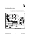
Chapter 3 Hardware Overview
© National Instruments Corporation 3-9 NI 6115/6120 User Manual
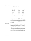
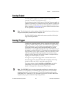
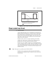
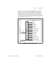
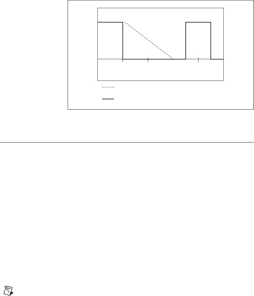
Figure 3-9. Effects of Hardware and Software Filtering on Antialiasing
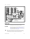
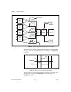
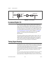
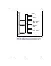
Phase-Locked Loop Circuit
♦ NI PXI-6115/6120
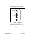
A phase-locked loop (PLL) circuit accomplishes the synchronization of
multiple NI PXI-6115/6120 devices or other PXI devices which support
PLL synchronization by allowing these devices to all lock to the same
reference clock present on the PXI backplane. This circuit allows you to
trigger input or output operations on different devices and ensures that
samples occur at the same time.
The PLL circuitry consists of a voltage-controlled crystal oscillator
(VCXO) with a tuning range of ±50 ppm. The VCXO generates the
60 MHz master clock used onboard the NI PXI-6115/6120.
The PLL locks to the 10 MHz oscillator line on the PXI backplane bus.
A phase comparator running at 1 MHz compares the PXI Bus and VCXO
clock. The loop filter then processes the error signal and outputs a control
voltage for the VCXO. Figure 3-10 illustrates the block diagram for the
NI PXI-6115/6120.
Note This feature is not available on the NI PCI-6115/6120.
The PLL circuit is automatically enabled when the NI 6115/6120 is
powered up. No configuration steps are required in order to utilize PLL
synchronization.
f
cutoff
f
Nyquist
(2 f
cutoff
)
4 f
cutoff
Response of Analog Hardware Filters
Response of Software Filters