


Operation DMD15/DMD15L IBS/IDR Satellite Modem
3-4 TM051 – Rev. 5.8
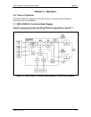
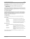
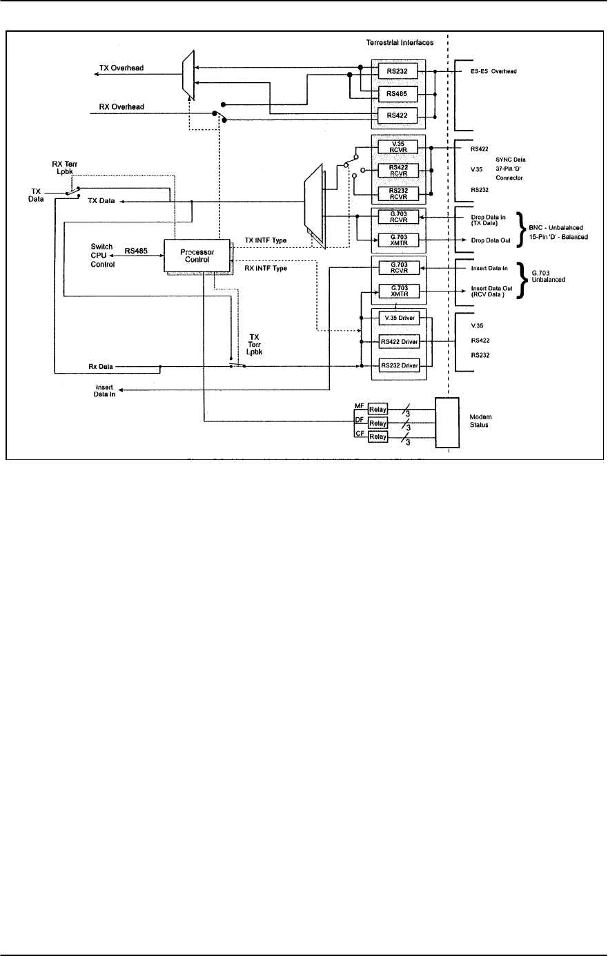
Figure 3-3. Universal Interface Modules (UIM) Functional Block Diagram
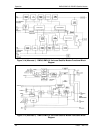
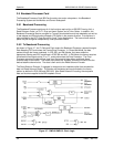
3.3 Synchronous Interface
Synchronous Tx Data and Clock enters the UIM and is routed to either the RS-422, RS-232, or
V.35 Receiver as the selected M&C Processor. The signals are then converted to an RS-422
balanced format and sent to the Baseband (BB) Processor Card. Receive Data from the BB
Processor Card undergoes the reverse process where it is converted from RS-422 Balanced
format and routed to the RS-422 or V.35 Drivers.
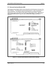
3.4 G.703 Interface
Either Balanced or Unbalanced G.703 Data is routed from the ‘Send Data In’ Connections to the
G.703 Receiver. The G.703 Receiver recovers a clock from the data stream, converts the clock
and data to an RS-422 balanced format, and routes the clock and data to the BB Processor. The
reverse process is performed on the Receive Data Stream where the G.703 Data exits the
modem at the ‘Receive Data Out’ Connection. The G.703 Interface is designed to operate at the
following data rates:
T1 (1.544 Mbps)
E1 (2.048 Mbps)
T2 (6.312 Mbps)
E2 (8.448 Mbps)
Additionally, the line code is selected when the interface type is selected with the exception that
T1 may use B8ZS or AMI as selected at the Front Panel.
The G.703 Interface also contains two additional ports that can operate at T1 or E1 that provides
a four port D&I Interface. The ‘Drop Data Out’ Port provides an unaltered Send Data Output that
can be used for daisy chaining additional systems. On the receive side, a T1 or E1 Data Stream