


Rev.1.10 Jul 01, 2005 page 87 of 318
REJ09B0124-0110
M16C/6N Group (M16C/6NK, M16C/6NM) 11. DMAC
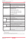
Under development
This document is under development and its contents are subject to change.
11.1 Transfer Cycle
The transfer cycle consists of a memory or SFR read (source read) bus cycle and a write (destination write)
bus cycle. The number of read and write bus cycles is affected by the source and destination addresses of
transfer. The bus cycle itself is extended by a software wait.
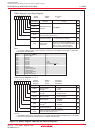
11.1.1 Effect of Source and Destination Addresses
If the transfer unit and data bus both are 16 bits and the source address of transfer begins with an odd
address, the source read cycle consists of one more bus cycle than when the source address of transfer
begins with an even address.
Similarly, if the transfer unit and data bus both are 16 bits and the destination address of transfer begins
with an odd address, the destination write cycle consists of one more bus cycle than when the destination
address of transfer begins with an even address.
11.1.2 Effect of Software Wait
For memory or SFR accesses in which one or more software wait states are inserted, the number of bus
cycles required for that access increases by an amount equal to software wait states.
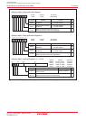
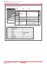
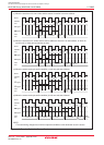
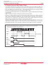
Figure 11.5 shows the example of the cycles for a source read. For convenience, the destination write cycle
is shown as one cycle and the source read cycles for the different conditions are shown. In reality, the
destination write cycle is subject to the same conditions as the source read cycle, with the transfer cycle
changing accordingly. When calculating transfer cycles, take into consideration each condition for the
source read and the destination write cycle, respectively. For example, when data is transferred in 16- bit unit
using an 8-bit bus ((2) on Figure 11.5), two source read bus cycles and two destination write bus cycles are
required.