


Rev.1.10 Jul 01, 2005 page 36 of 318
REJ09B0124-0110
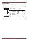
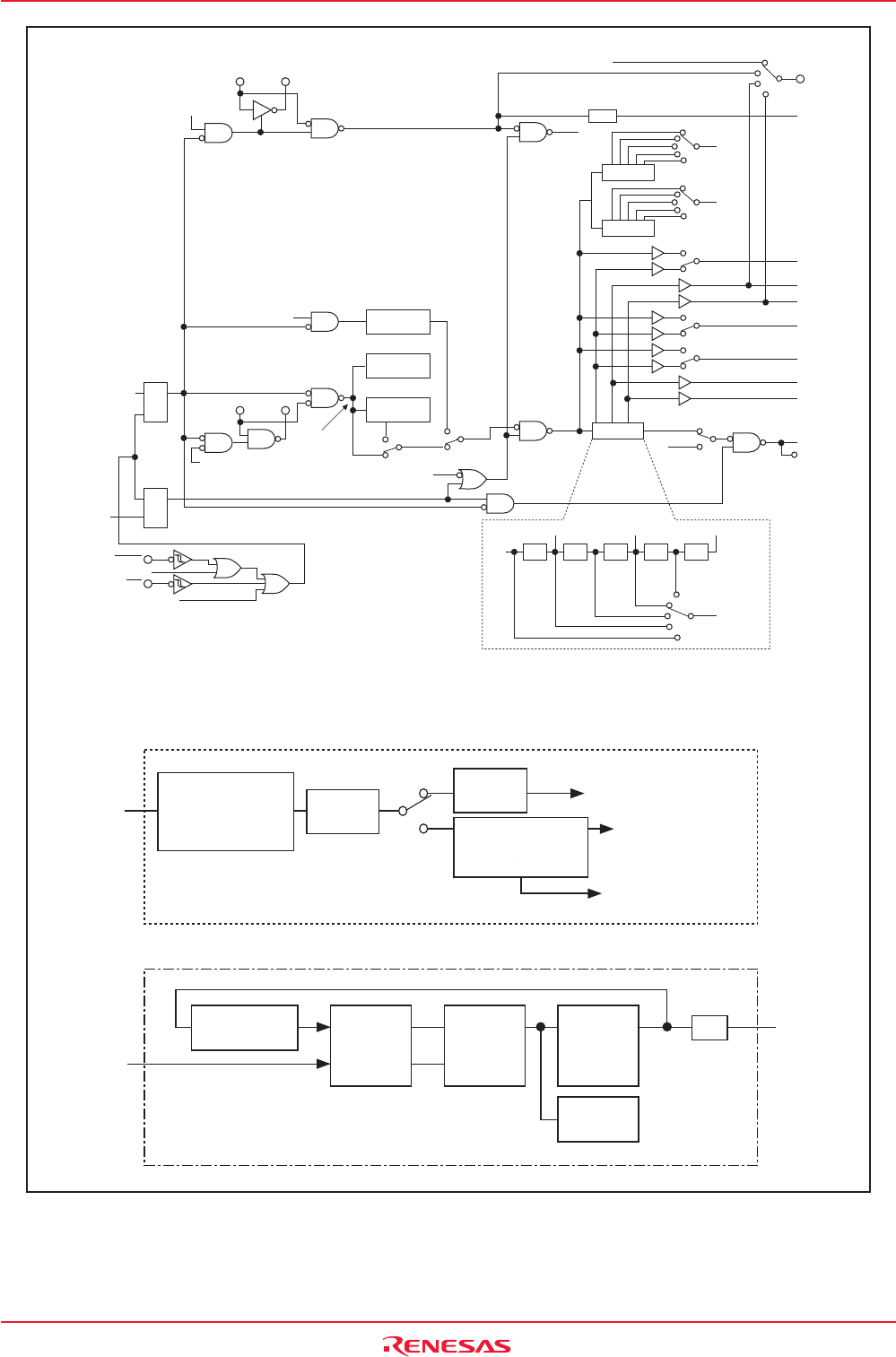
M16C/6N Group (M16C/6NK, M16C/6NM) 7. Clock Generating Circuit
Under development
This document is under development and its contents are subject to change.
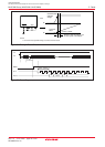
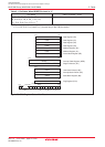
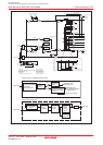
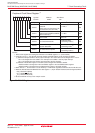
Figure 7.1 Clock Generating Circuit
1/16
CLKOUT
CM01-CM00=00b
PM01-PM00=00b, CM01-CM00=01b
PM01-PM00=00b, CM01-CM00=10b
PM01-PM00=00b,
CM01-CM00=11b
I/O ports
1/32
fC32
f
1
f
2
f
AD
PCLK0=1
PCLK0=0
PCLK0=1
PCLK0=0
f
1SIO
f
2SIO
PCLK1=1
PCLK1=0
CM07=0
CPU clock
BCLK
CM07=1
f
C
f
8
f
32
f
8SIO
f
32SIO
Divider
bcd
e
a
CM21=1
CM21=0
1
0 CM11
PLL frequency
synthesizer
Oscillation stop,
re-oscillation
detection circuit
On-chip
oscillator
XOUTXIN
Main clock
oscillation circuit
Main clock
CM05
XCOUTXCIN
Sub clock oscillation circuit
CM04
PLL clock
On-chip oscillator
clock
CM02
QS
R
QS
R
CM10=1
(stop mode)
WAIT instruction
RESET
NMI
Software reset
Interrupt request level
judgment output
1/2 1/2 1/2 1/2 1/2
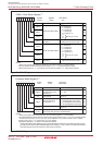
Details of divider
b
1/81/41/2
a
1/32
CM06=0
CM17-CM16=11b
CM06=0
CM17-CM16=10b
CM06=1
CM06=0
CM17-CM16=01b
CM06=0
CM17-CM16=00b
PM00, PM01 : Bits in PM0 register
CM00, CM01, CM02, CM04, CM05, CM06, CM07 : BIts in CM0 register
CM10, CM11, CM16, CM17 : Bits in CM1 register
PCLK0, PCLK1 : Bits in PCLKR register
CM21, CM27 : Bits in CM2 register
CCLK0 to CCLK2, CCLK4 to CCLK6 : Bits in CCLKR register
Sub clock
CM21
f
C
e
cd
f
CAN1
By CCLK0,1 and 2
By CCLK4,5 and 6
fCAN0
Divider
Divider
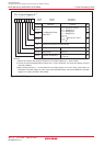
Reset
generating
circuit
Oscillation stop,
re-oscillation detection
interrupt generating
circuit
Main clock
Oscillation stop
detection reset
CM21 switch signal
Oscillation stop,
re-oscillation detection
interrupt signal
Oscillation stop, re-oscillation detection circuit
Charge,
discharge
circuit
Pulse generating circuit
for clock edge detection
and charge,
discharge control
CM27 = 0
CM27 = 1
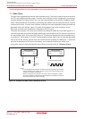
Main clock
PLL clock
PLL frequency synthesizer
Phase
comparator
Voltage
control
oscillator
(VCO)
Internal
lowpass filter
Charge
pump
Programmable
counter
1/2