


Rev.1.10 Jul 01, 2005 page 2 of 318
REJ09B0124-0110
M16C/6N Group (M16C/6NK, M16C/6NM) 1. Overview
Under development
This document is under development and its contents are subject to change.
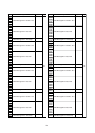
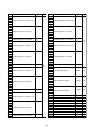
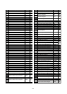
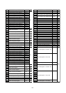
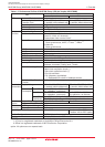
1.2 Performance Outline
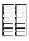
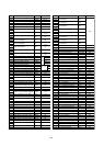
Tables 1.1 and 1.2 list a performance outline of M16C/6N Group (M16C/6NK, M16C/6NM).
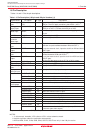
Table 1.1 Performance Outline of M16C/6N Group (100-pin Version: M16C/6NK)
Item
Performance
Normal-ver. T/V-ver.
CPU Number of Basic Instructions 91 instructions
Minimum Instruction 41.7ns (f(BCLK) = 24MHz, 50.0ns (f(BCLK) = 20MHz,
Execution Time
1/1 prescaler, without software wait) 1/1 prescaler, without software wait)
Operation Mode Single-chip mode
Address Space 1 Mbyte
Memory Capacity See Table 1.3 Product List
Peripheral Port Input/Output: 87 pins, Input: 1 pin
Function Multifunction Timer Timer A: 16 bits ✕ 5 channels
Timer B: 16 bits ✕ 6 channels
Three-phase motor control circuit
Serial I/O 3 channels
Clock synchronous, UART, I
2
C-bus
(1)
, IEBus
(2)
2 channels
Clock synchronous
A/D Converter 10-bit A/D converter: 1 circuit, 26 channels
D/A Converter 8 bits ✕ 2 channels
DMAC 2 channels
CRC Calculation Circuit CRC-CCITT
CAN Module 2 channels with 2.0B specification
Watchdog Timer 15 bits ✕ 1 channel (with prescaler)
Interrupt Internal: 32 sources, External: 9 sources
Software: 4 sources, Priority level: 7 levels
Clock Generating Circuit 4 circuits
• Main clock oscillation circuit (*)
• Sub clock oscillation circuit (*)
• On-chip oscillator
• PLL frequency synthesizer
(*) Equipped with a built-in feedback resistor
Oscillation Stop Detection Main clock oscillation stop and re-oscillation detection function
Function
Electrical Supply Voltage
VCC = 3.0 to 5.5V (f(BCLK) = 24MHz, VCC = 4.2 to 5.5V (f(BCLK) = 20MHz,
Characteristics
1/1 prescaler, without software wait) 1/1 prescaler, without software wait)
Power Mask ROM 21mA (f(BCLK) = 24MHz, -
Consumption PLL operation, no division)
Flash Memory
23mA (f(BCLK) = 24MHz, 21mA (f(BCLK) = 20MHz,
PLL operation, no division) PLL operation, no division)
Mask ROM 3µA
(f(BCLK) = 32kHz, Wait mode, Oscillation capacity Low)
Flash Memory
0.8µA (Stop mode, Topr = 25°C)
Flash Memory Program/Erase Supply Voltage
3.0 ± 0.3V or 5.0 ± 0.5V 5.0 ± 0.5V
Version
Program and Erase Endurance
100 times
I/O I/O Withstand Voltage 5.0V
Characteristics
Output Current 5mA
Operating Ambient Temperature -40 to 85°C T version: -40 to 85°C
V version: -40 to 125°C
(option)
Device Configuration CMOS high performance silicon gate
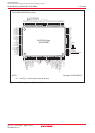
Package 100-pin plastic mold LQFP
NOTES:
1. I
2
C-bus is a registered trademark of Koninklijke Philips Electronics N.V.
2. IEBus is a registered trademark of NEC Electronics Corporation.
option: All options are on request basis.