


Rev.1.10 Jul 01, 2005 page 41 of 318
REJ09B0124-0110
M16C/6N Group (M16C/6NK, M16C/6NM) 7. Clock Generating Circuit
Under development
This document is under development and its contents are subject to change.
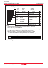
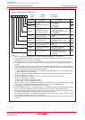
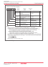
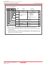
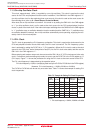
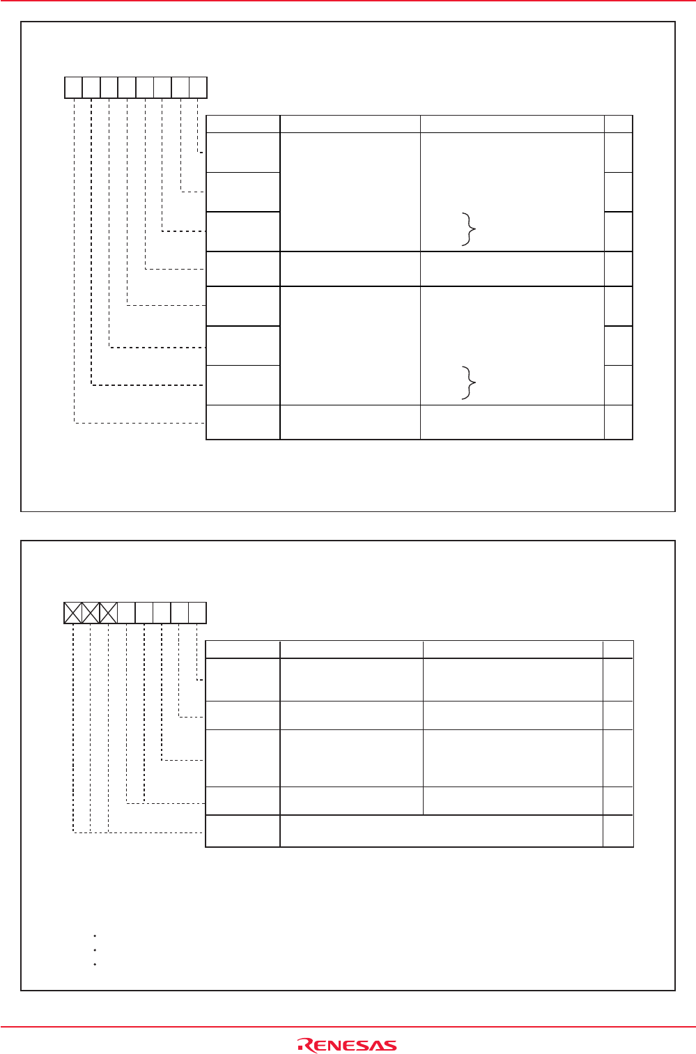
Symbol Address After Reset
PM2 001Eh XXX00000b
Processor Mode Register 2
(1)
b7 b6 b5 b4 b3 b2 b1 b0
000
Specifying Wait when
Accessing SFR at PLL
Operation
(2)
0 : 2 waits
1 : 1 wait
Nothing is assigned. When write, set to "0".
When read, their contents are indeterminate.
Reserved Bit
RW
RW
RW
RW
-
WDT Count Source
Protective Bit
(3) (4)
0 : CPU clock is used for the
watchdog timer count source
1 : On-chip oscillator clock is used for
the watchdog timer count source
Reserved Bit Set to "0"
Set to "0"
Bit Name Function
Bit Symbol
RW
PM20
-
(b1)
-
(b4-b3)
-
(b7-b5)
PM22
NOTES:
1. Write to this register after setting the PRC1 bit in the PRCR register to "1" (write enable).
2. The PM20 bit become effective when the PLC07 bit in the PLC0 register is set to "1" (PLL on). Change the PM20
bit when the PLC07 bit is set to "0" (PLL off). Set the PM20 bit t "0" (2 waits) when PLL clock > 16MHz.
3. Once this bit is set to "1", it cannot be set to "0" in a program.
4. Setting the PM22 bit to "1" results in the following conditions:
The on-chip oscillator starts oscillating, and the on-chip oscillator clock becomes the watchdog timer count source.
The CM10 bit in the CM1 register is disabled against write. (Writing a "1" has no effect, nor is stop mode entered.)
The watchdog timer does not stop when in wait mode or hold state.
Figure 7.7 PM2 Register
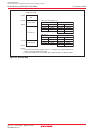
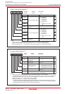
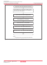
Figure 7.6 CCLKR Register
RW
RW
RW
RW
0 0 0 No division
0 0 1 : Divide-by-2
0 1 0 : Divide-by-4
0 1 1 : Divide-by-8
1 0 0: Divide-by-16
1 0 1 :
1 1 0 : Do not set a value
1 1 1 :
b2 b1 b0
CAN0 Clock Select Bits
(2)
CAN0 CPU Interface
Sleep Bit
(3)
0: CAN0 CPU interface operating
1: CAN0 CPU interface in sleep
Bit Name FunctionBit Symbol
RW
CCLK3
CCLK1
CCLK2
CCLK0
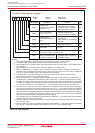
Symbol Address After Reset
CCLKR 025Fh 00h
CAN0/1 Clock Select Register
(1)
b7 b6 b5 b4 b3 b2 b1 b0
RW
RW
RW
RW
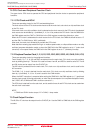
0 0 0 No division
0 0 1 : Divide-by-2
0 1 0 : Divide-by-4
0 1 1 : Divide-by-8
1 0 0: Divide-by-16
1 0 1 :
1 1 0 : Do not set a value
1 1 1 :
b6 b5 b4
CAN1 Clock Select Bits
(2)
CAN1 CPU Interface
Sleep Bit
(3)
0: CAN1 CPU interface operating
1: CAN1 CPU interface in sleep
CCLK7
CCLK5
CCLK6
CCLK4
NOTES:
1. Write to this register after setting the PRC0 bit in the PRCR register to "1" (Write enabled).
2. Set only when the Reset bit in the CiCTLR register (i = 0, 1) = 1 (Reset/Initialization mode).
3. Before setting this bit to "1", set the Sleep bit in the CiCTLR register to "1" (Sleep mode enabled).