


Rev.1.10 Jul 01, 2005 page 176 of 318
REJ09B0124-0110
M16C/6N Group (M16C/6NK, M16C/6NM) 14. Serial I/O
Under development
This document is under development and its contents are subject to change.
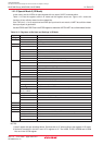
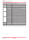
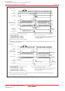
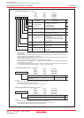
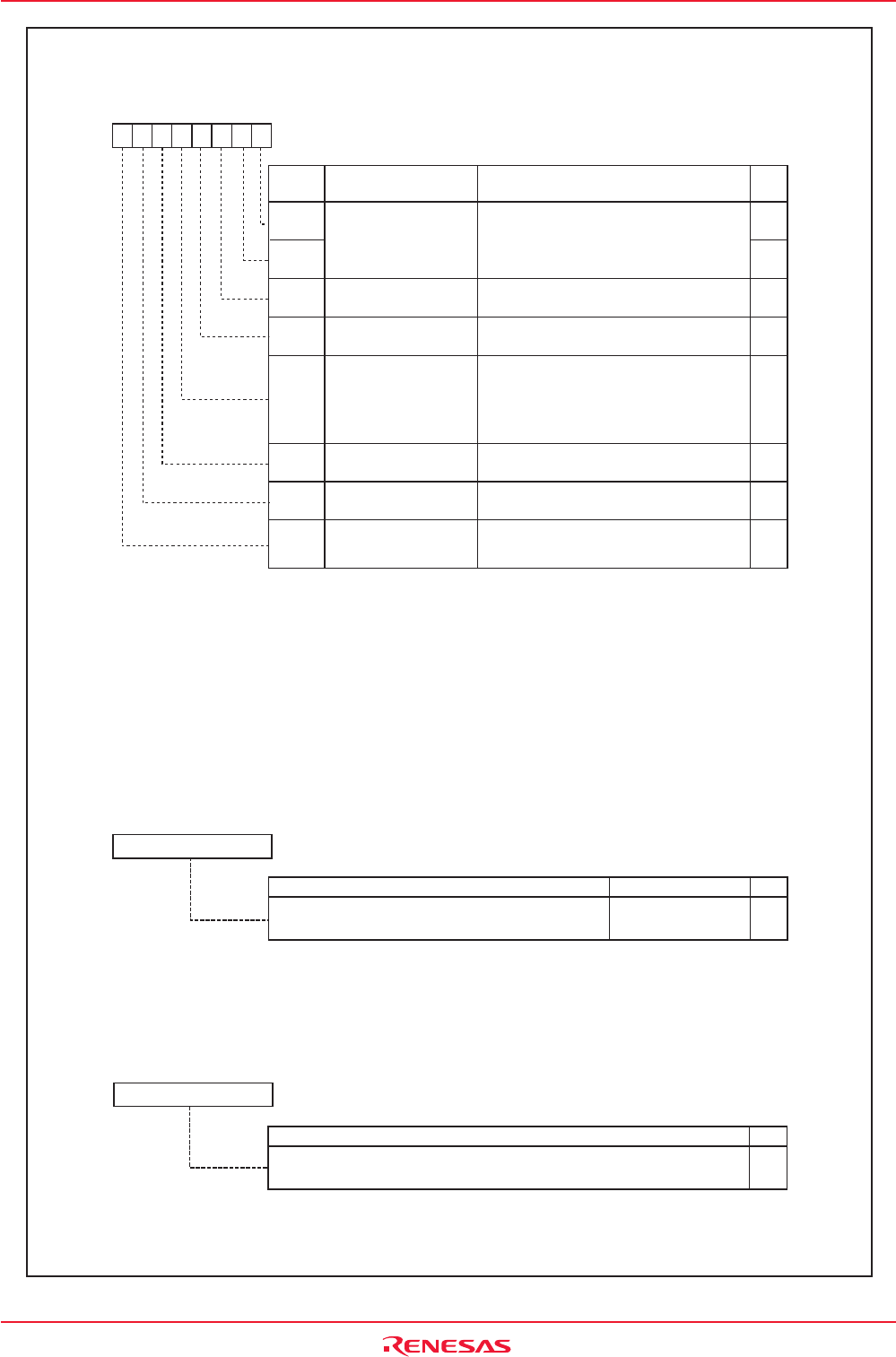
Figure 14.37 S3C to S6C Registers, S3BRG to S6BRG Registers, and S3TRR to S6TRR Registers
0 0 : Selecting f1SIO or f2SIO
0 1 : Selecting f8SIO
1 0 : Selecting f32SIO
1 1 : Do not set a value
0 : Input/output port
1 : SOUTi output, CLKi function
0 : SOUTi output
1 : SOUTi output disabled (high-impedance)
0 : Transmit data is output at falling edge of
transfer clock and receive data is input
at rising edge
1 : Transmit data is output at rising edge of
transfer clock and receive data is input
at falling edge
b1 b0
0 : LSB first
1 : MSB first
0 : External clock
(2)
1 : Internal clock
(3)
Effective when the SMi3 bit = 0
0 : "L" output
1 : "H" output
b7 b6 b5 b4 b3 b2 b1 b0
SI/Oi Control Register (i = 3 to 6)
(1)
Symbol Address After Reset
S3C
S4C
S5C
(6)
S6C
(6)
01E2h
01E6h
01EAh
01D8h
01000000b
01000000b
01000000b
01000000b
Bit
Symbol
Bit Name
Description
RW
RW
RW
RW
RW
RW
RW
RW
RW
SMi5
SMi1
SMi0
SMi3
SMi6
SMi7
SMi2
SMi4
Internal Synchronous
Clock Select Bit
Transfer Direction Select
Bit
S I/Oi Port Select Bit
(5)
SOUTi Initial Value Set Bit
Synchronous Clock
Select Bit
SOUTi Output Disable
Bit
(4)
CLK Polarity Select Bit
NOTES:
1.Make sure this register is written to by the next instruction after setting the PRC2 bit in the PRCR register to "1"
(write enabled).
2. Set the SMi3 bit to "1" (SOUTi output, CLKi function) and the corresponding port direction bit to "0" (input mode).
3. Set the SMi3 bit to "1" (SOUTi output, CLKi function).
4.When the SM32, SM52 or SM62 bit = 1, the corresponding pin is placed in the high-impedance state regardless of
which functions of those pins are being used.
SI/O4 is effective only when the SM43 bit = 1 (SOUT4 output, CLK4 function).
5.When using SI/O4, set the SM43 bit to "1" (SOUT4 output, CLK4 function) and the corresponding port direction bit
for SOUT4 pin to "0" (input mode).
6. The S5C and S6C registers are only in the 128-pin version. When using the S5C and S6C registers, set these registers
after setting the PU37 bit in the PUR3 register to "1" (Pins P11 to P14 are usable).
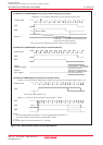
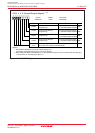
NOTES:
1. Write to this register while serial I/O is neither transmitting nor receiving.
2. Use the MOV instruction to write to this register.
3. The S5BRG and S6BRG registers are only in the 128-pin version.
Description
RW
WO
Assuming that set value = n, SiBRG divides the count
source by n + 1
Symbol Address After Reset
S3BRG
S4BRG
S5BRG
(3)
S6BRG
(3)
01E3h
01E7h
01EBh
01D9h
Indeterminate
Indeterminate
Indeterminate
Indeterminate
b7 b0
00h to FFh
Setting Range
SI/Oi Bit Rate Generator (i = 3 to 6)
(1) (2)
NOTES:
1. Write to this register while serial I/O is neither transmitting nor receiving.
2. To receive data, set the corresponding port direction bit for SINi to "0" (input mode).
3. The S5TRR and S6TRR registers are only in the 128-pin version.
b7 b0
Symbol Address After Reset
S3TRR
S4TRR
S5TRR
(3)
S6TRR
(3)
01E0h
01E4h
01E8h
01D6h
Indeterminate
Indeterminate
Indeterminate
Indeterminate
RW
RW
Description
SI/Oi Transmit/Receive Register (i = 3 to 6)
(1) (2)
Transmission/reception starts by writing transmit data to this register.
After transmission/reception finishes, reception data can be read by reading this register.