


( 17 / 84 )
IMPORTANT
Note on Reading Internal Resources of the MCU:
• When the registers that are listed in Table 1.1 are read with an emulator, those results will be the
following (the data in the MCU are not effected).
(1) Results of real-time trace
The data values of the cycles read are not displayed correctly.
(2) Real-time RAM monitor
The data values read are not displayed correctly.
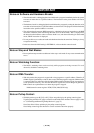
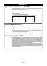
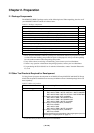
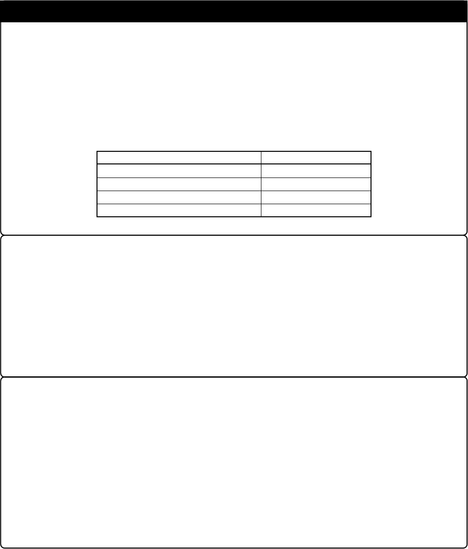
Table 1.1 Resisters and symbols not displayed normally (*1: M16C/62N only)
Note on Protect Register (PRC2):
•Make note of the fact that the protect is not canceled when protect register (PRC2), which enables
writing in the port P9 direction register and the SI/Oi control register, is changed with the below
procedure.
(1) Step execution of the "instruction for setting ("1") PRC2"
(2) Setting the break point from the instruction for setting ("1") PRC2 to when the port P9
direction register and SI/Oi control register are set.
(3) Setting "("1") PRC2" from the dump window or script window
Note on Accessing Address 00000h:
• With M16C/60 Series MCUs, when a maskable interrupt is generated, the interrupt data (interrupt
No. and interrupt request level) stored in address 00000h is read out. Also, the interrupt request bit
is cleared when address 00000h is read out. Consequently, when the address 00000h readout
instruction is executed or when address 00000h is read out in the cause of a program runaway, a
malfunction occurs in that the interrupt is not executed despite the interrupt request, because the
request bit of the highest priority interrupt factor enabled is cleared.
For this malfunction, when the reading out to the address 00000h is generated excluding the
interrupt, the yellow LED lights up to alarm. When this LED lights, there is a possibility of wrong
access to address 00000h, therefore check the program. This LED is turned off by the system reset
switch of the emulator main unit.
Resister Symbol
DMA source pointers 0, 1 (*1) SAR0, SAR1 (*1)
DMA destination pointers 0, 1 (*1) DAR0, DAR1 (*1)
DMA transfer counters 0, 1 (*1) TCR0, TCR1 (*1)
DMA control resisters 0, 1 (*1) DM0CON, DM1CON (*1)