


( 67 / 84 )
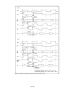
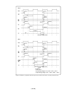
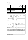
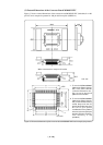
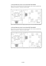
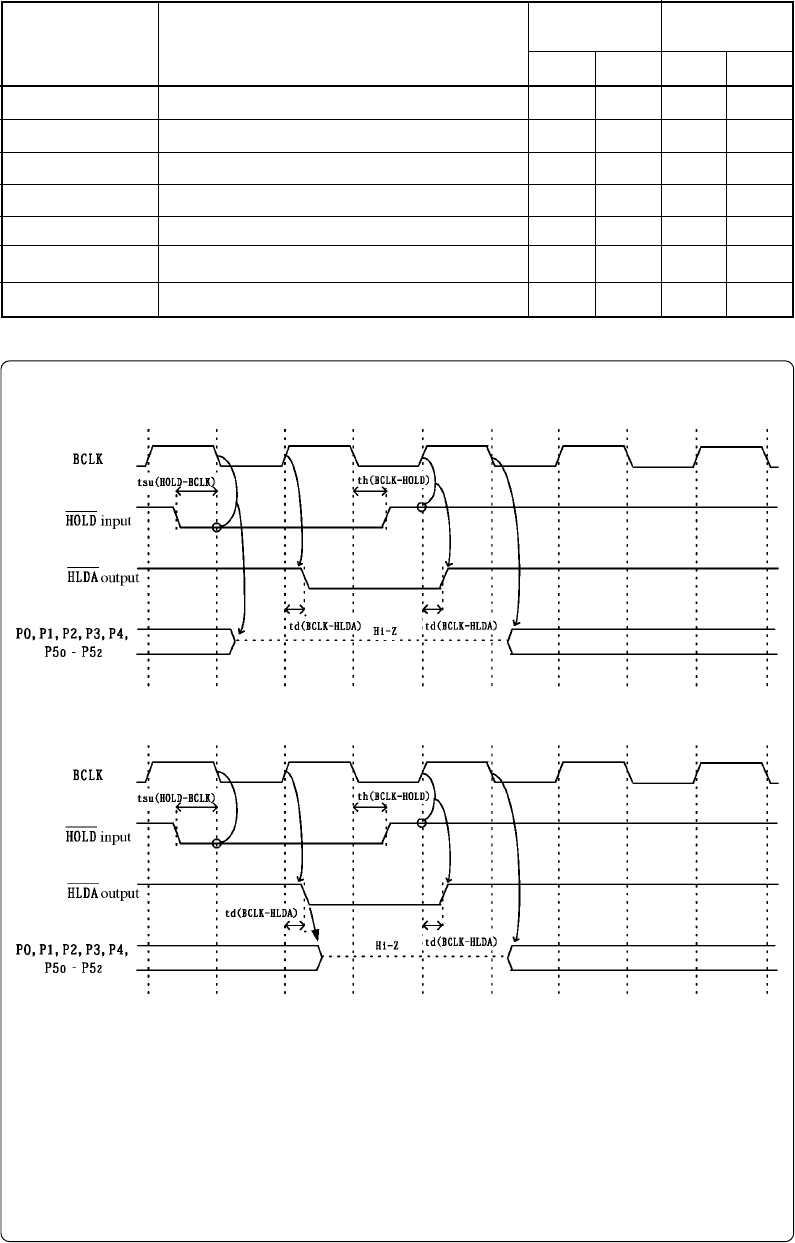
Figure 5.4 Timing requirements
(4) Timing Requirements
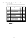
Table 5.5 and Figure 5.4 show the timing requirements.
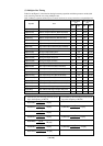
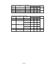
Table 5.5 Timing requirements
Common to "with wait" and "no-wait" (this product)
Common to "with wait" and "no-wait" (actual MCU)
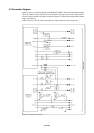
Note 1. P00 to P52 will be high-impedance status regardless of the input level of pin BYTE and ports
P40 to P43 function selection bit (PM06) of the processor mode register 0.
Note 2. Compared with the actual MCU, this product enters high-impedance state after a 0.5 cycle
delay.
Conditions:
• VCC = 3.3 V
• Input timing voltage: VIL = 0.66 V, VIH = 2.64 V
• Output timing voltage: VOL = 1.65 V, VOH = 1.65 V
Symbol Item
Actual MCU
[ns]
This product
[ns]
Min. Max.
Min.
Max.
tsu(DB-RD)
tsu(RDY-BCLK)
tsu(HOLD-BCLK)
th(RD-DB)
th(BCLK-RDY)
th(BCLK-HOLD)
td(BCLK-HLDA)
Data input setup time
RDY* input setup time
HOLD* input setup time
Data input hold time
RDY* input hold time
HOLD* input hold time
HLDA* output delay time
50
50
100
0
0
0
40
65
65
115
See left
See left
See left
See left