


Si5351A/B/C
Preliminary Rev. 0.95 15
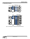
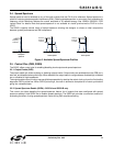
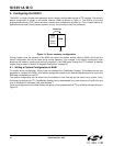
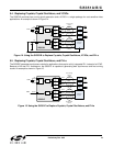
Figure 9. I
2
C Write Operation
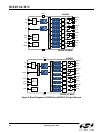
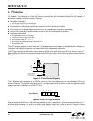
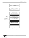
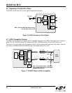
A read operation is performed in two stages. A data write is used to set the register address, then a data read is
performed to retrieve the data from the set address. A read burst operation is also supported. This is shown in
Figure 10.
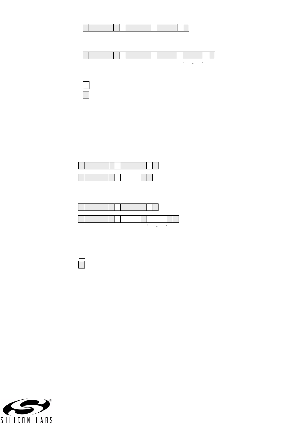
Figure 10. I
2
C Read Operation
AC and DC electrical specifications for the SCL and SDA pins are shown in Table 7. The timing specifications and
timing diagram for the I
2
C bus is compatible with the I
2
C-Bus Standard. SDA timeout is supported for compatibility
with SMBus interfaces.
1 – Read
0 – Write
A – Acknowledge (SDA LOW)
N – Not Acknowledge (SDA HIGH)
S – START condition
P – STOP condition
From slave to master
From master to slave
Write Operation – Single Byte
S 0 A Reg Addr [7:0]Slv Addr [6:0] A Data [7:0] PA
Write Operation - Burst (Auto Address Increment)
Reg Addr +1
S 0 A Reg Addr [7:0]Slv Addr [6:0] A Data [7:0] A Data [7:0] PA
1 – Read
0 – Write
A – Acknowledge (SDA LOW)
N – Not Acknowledge (SDA HIGH)
S – START condition
P – STOP condition
From slave to master
From master to slave
Read Operation – Single Byte
S 0 A Reg Addr [7:0]Slv Addr [6:0] A P
Read Operation - Burst (Auto Address Increment)
Reg Addr +1
S 1 ASlv Addr [6:0] Data [7:0] PN
S 0 A Reg Addr [7:0]Slv Addr [6:0] A P
S 1 ASlv Addr [6:0] Data [7:0] A PNData [7:0]