


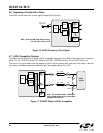
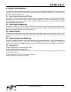
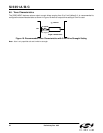
Si5351A/B/C
24 Preliminary Rev. 0.95
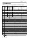
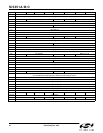
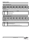
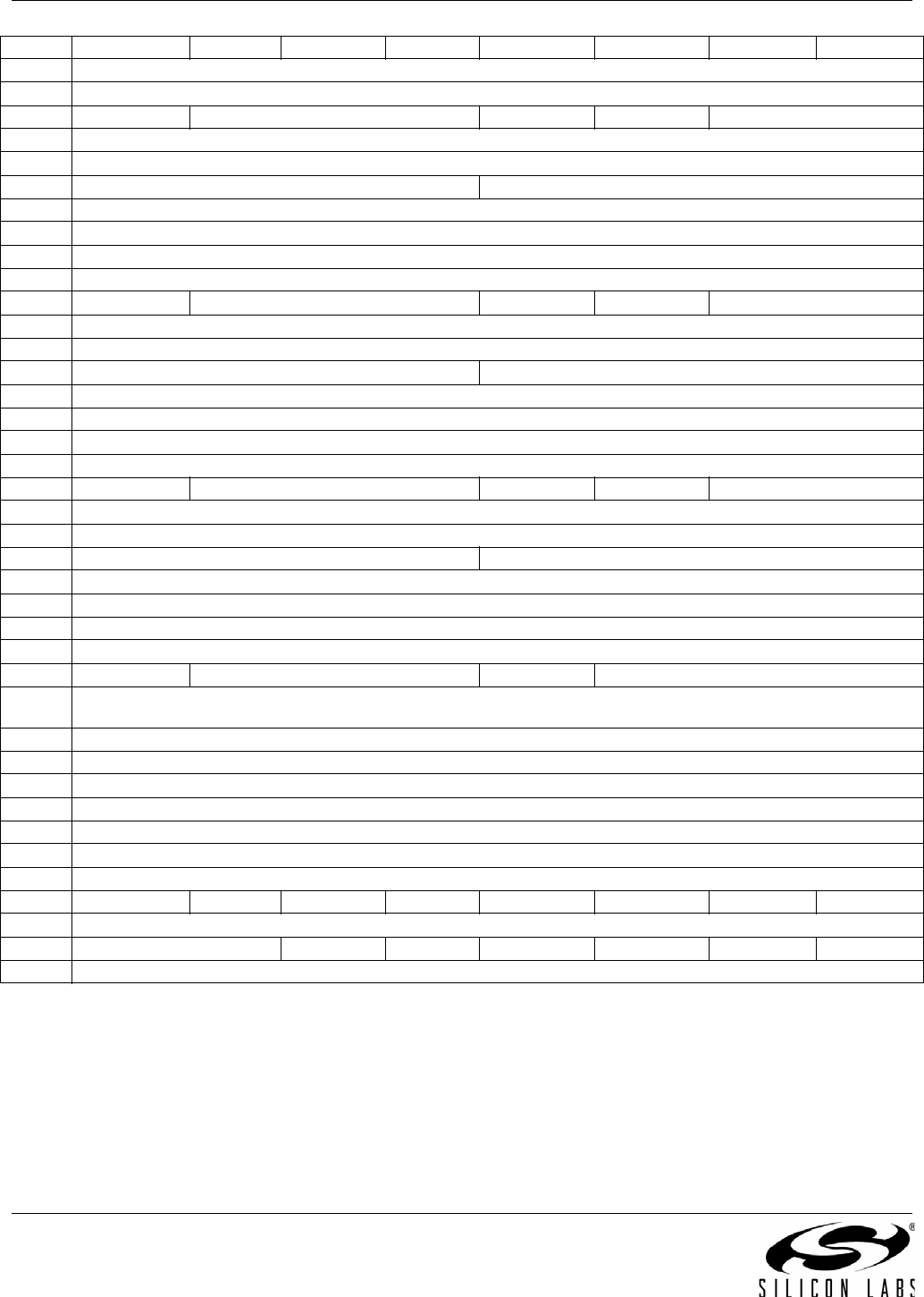
66 MS3_P3[15:8]
67 MS3_P3[7:0]
68 R3_DIV[2:0] MS3_P1[17:16]
69 MS3_P1[15:8]
70 MS3_P1[7:0]
71 MS3_P3[19:16] MS3_P2[19:16]
72 MS3_P2[15:8]
73 MS3_P2[7:0]
74 MS4_P3[15:8]
75 MS4_P3[7:0]
76 R4_DIV[2:0] MS4_P1[17:16]
77 MS4_P1[15:8]
78 MS4_P1[7:0]
79 MS4_P3[19:16] MS4_P2[19:16]
80 MS4_P2[15:8]
81 MS4_P2[7:0]
82 MS5_P3[15:8]
83 MS5_P3[7:0]
84 R5_DIV[2:0] MS5_P1[17:16]
85 MS5_P1[15:8]
86 MS5_P1[7:0]
87 MS5_P3[19:16] MS5_P2[19:16]
88 MS5_P2[15:8]
89 MS5_P2[7:0]
90 MS6_P1[7:0]
91 MS7_P1[7:0]
92 R7_DIV[2:0] R6_DIV[2:0]
93–164 PLL, MultiSynth, and output clock delay offset Configuration Registers.
Use ClockBuilder Desktop Software to Determine These Register Values.
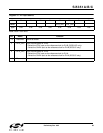
165 CLK0_PHOFF[7:0]
166 CLK1_PHOFF[7:0]
167 CLK2_PHOFF[7:0]
168 CLK3_PHOFF[7:0]
189 CLK4_PHOFF[7:0]
170 CLK5_PHOFF[7:0]
173–176 Reserved
177 PLLB_RST PLLA_RST
178–182 Reserved
183 XTAL_CL
184–255 Reserved
Register 7 6 5 4 3 2 1 0