


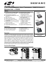
Si5351A/B/C
Preliminary Rev. 0.95 5
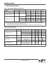
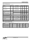
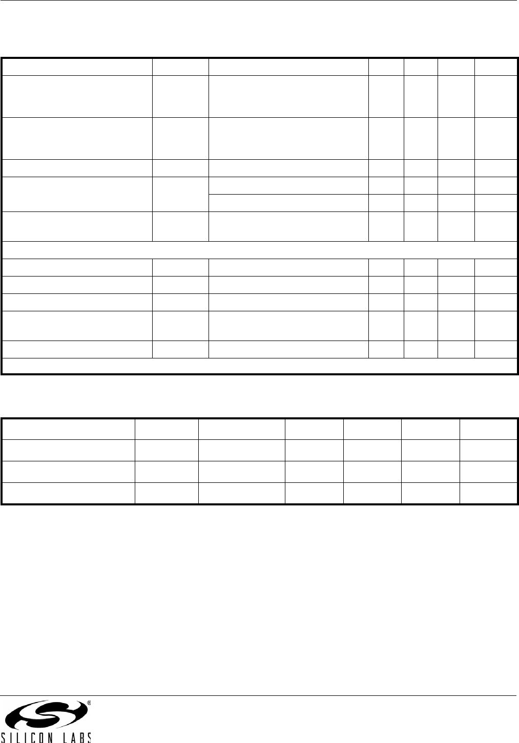
Table 3. AC Characteristics
(V
DD
= 2.5 V ±10%, or 3.3 V ±10%, T
A
= –40 to 85 °C)
Parameter Symbol Test Condition Min Typ Max Unit
Power-up Time T
RDY
From V
DD
=V
DDmin
to valid
output clock, C
L
=5pF,
f
CLKn
>1MHz
—110ms
Output Enable Time T
OE
From OEB pulled low to valid
clock output, C
L
=5pF,
f
CLKn
>1MHz
——10 µs
Output Phase Offset P
STEP
— 333 — ps/step
Spread Spectrum Frequency
Deviation
SS
DEV
Down spread –0.1 — –2.5 %
Center spread ±0.1 — ±1.5 %
Spread Spectrum Modulation
Rate
SS
MOD
30 31.5 33 kHz
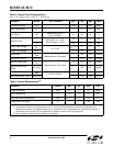
VCXO Specifications (Si5351B only)
VCXO Control Voltage Range Vc 0 V
DD
/2 V
DD
V
VCXO Gain (configurable) Kv Vc = 10–90% of V
DD
, V
DD
= 3.3 V 18 — 150 ppm/V
VCXO Control Voltage Linearity KVL Vc = 10–90% of V
DD
–5 — +5 %
VCXO Pull Range
(configurable)
PR V
DD
= 3.3 V* ±30 0 ±240 ppm
VCXO Modulation Bandwidth — 10 — kHz
*Note: Contact Silicon Labs for 2.5 V VCXO operation.
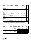
Table 4. Input Clock Characteristics
(V
DD
= 2.5 V ±10%, or 3.3 V ±10%, T
A
= –40 to 85 °C)
Parameter Symbol Test Condition Min Typ Max Units
CLKIN Input Low Voltage V
IL
–0.1 — 0.3 x V
DD
V
CLKIN Input High Voltage V
IH
0.7 x V
DD
—3.60 V
CLKIN Frequency Range f
CLKIN
10 — 100 MHz