


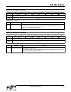
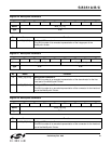
Si5351A/B/C
Preliminary Rev. 0.95 35
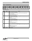
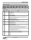
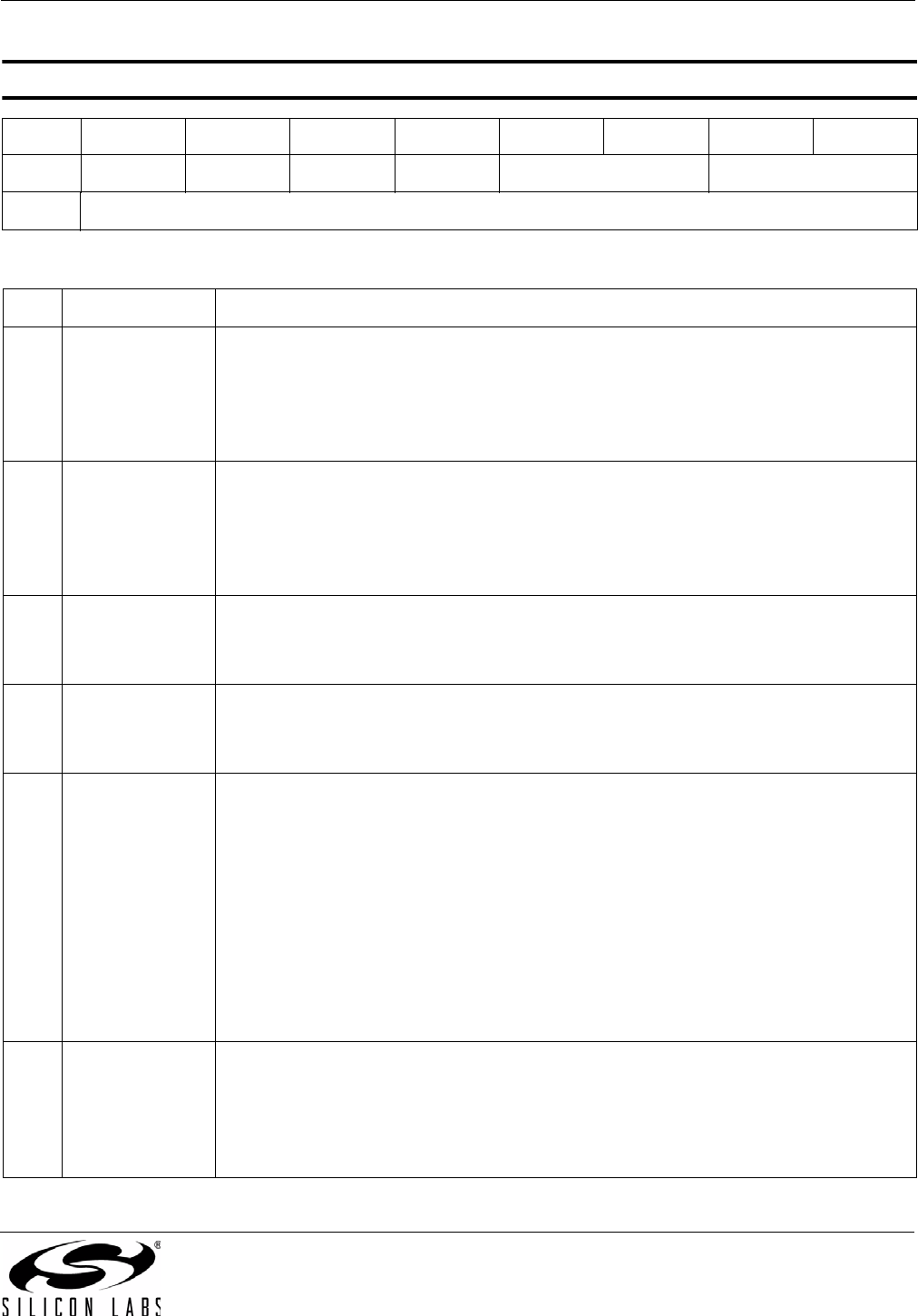
Reset value = 0000 0000
Register 21. CLK5 Control
BitD7D6D5D4D3D2D1D0
Name
CLK5_PDN MS5_INT MS5_SRC CLK5_INV CLK5_SRC[1:0] CLK5_IDRV[1:0]
Type
R/W R/W R/W R/W R/W R/W
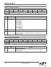
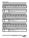
Bit Name Function
7 CLK5_PDN Clock 5 Power Down.
This bit allows powering down the CLK5 output driver to conserve power when the out-
put is unused.
0: CLK4 is powered up.
1: CLK4 is powered down.
6MS5_INTMultiSynth 5 Integer Mode.
This bit can be used to force MS5 into Integer mode to improve jitter performance.
Note that the fractional mode is necessary when a delay offset is specified for CLK4.
0: MS5 operates in fractional division mode.
1: MS5 operates in integer mode.
5MS5_SRCMultiSynth Source Select for CLK5.
0: Select PLLA as the source for MultiSynth0.
1: Select PLLB (Si5351A/C only) or VCXO (Si5351B only) MultiSynth0.
4 CLK5_INV Output Clock 5 Invert.
0: Output Clock 5 is not inverted.
1: Output Clock 5 is inverted.
3:2 CLK5_SRC[1:0] Output Clock 5 Input Source.
These bits determine the input source for CLK5.
00: Select the XTAL as the clock source for CLK5. This option by-passes both synthe-
sis stages (PLL/VCXO & MultiSynth) and connects CLK5 directly to the oscillator
which generates an output frequency determined by the XTAL frequency.
01: Select CLKIN as the clock source for CLK5. This by-passes both synthesis stages
(PLL/VCXO & MultiSynth) and connects CLK5 directly to the CLKIN input. This essen-
tially creates a buffered output of the CLKIN input.
10: Reserved. Do not select this option.
11: Select MultiSynth 0 as the source for CLK5. Select this option when using the
Si5351 to generate free-running or synchronous clocks.
1:0 CLK5_IDRV[1:0] CLK5 Output Rise and Fall time / Drive Strength Control.
00: 2 mA
01: 4 mA
10: 6 mA
11: 8 mA