


Si5351A/B/C
20 Preliminary Rev. 0.95
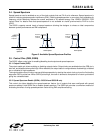
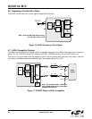
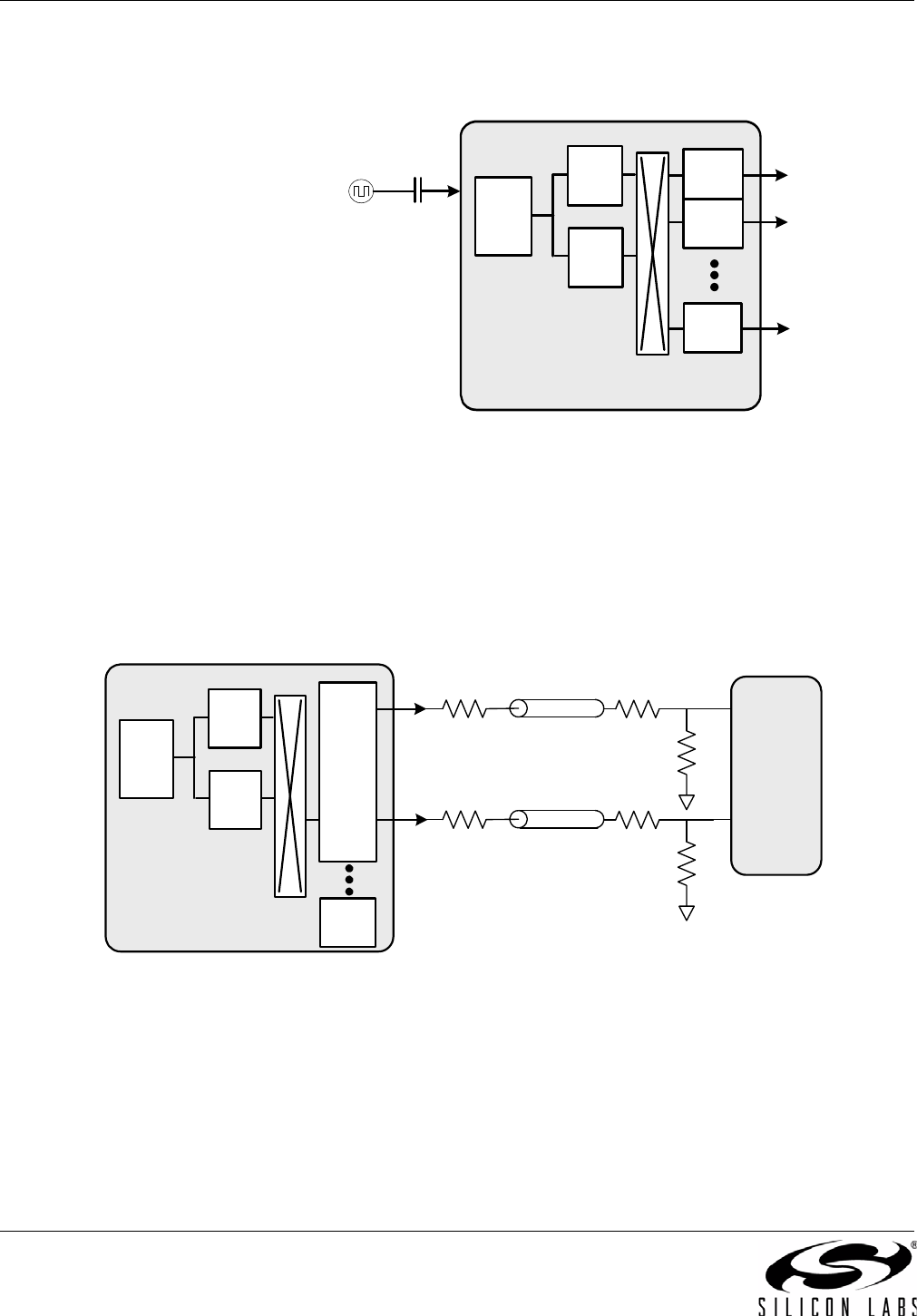
5.6. Replacing a Crystal with a Clock
The Si5351 can be driven with a clock signal through the XA input pin.
Figure 16. Si5351 Driven by a Clock Signal
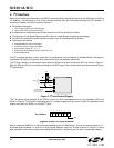
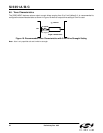
5.7. HCSL Compatible Outputs
The Si5351 can be configured to support HCSL compatible swing when the VDDO of the output pair of interest is
set to 2.5 V (i.e., VDDOA must be 2.5 V when using CLK0/1; VDDOB must be 2.5 V for CLK2/3 and so on).
The circuit in the figure below must be applied to each of the two clocks used, and one of the clocks in the pair
must also be inverted to generate a differential pair. See register setting CLKx_INV.
Figure 17. Si5350C Output is HCSL Compatible
Multi
Synth
N
Multi
Synth
0
Multi
Synth
1
PLLB
PLLA
XA
XB
OSC
V
IN
= 1 V
PP
25/27 MHz
Note: Float the XB input while driving
the XA input with a clock
0.1 µF
Multi
Synth
N
Multi
Synth
0
Multi
Synth
1
PLLB
PLLA
OSC
Note: The complementary -180 degree
out of phase output clock is generated
using the INV function
R
1
511
240
R
2
Z
O
= 70
0
HCSL
CLKIN
R
1
511
240
R
2
Z
O
= 70
0