


Si5351A/B/C
Preliminary Rev. 0.95 33
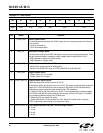
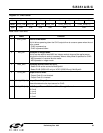
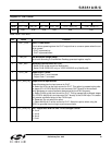
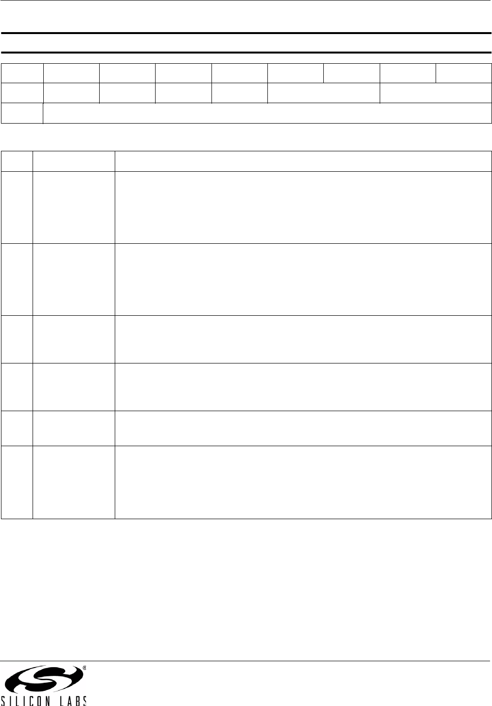
Reset value = 0000 0000
Register 19. CLK3 Control
BitD7D6D5D4D3D2D1D0
Name
CLK3_PDN MS3_INT MS3_SRC CLK3_INV CLK3_SRC[1:0] CLK3_IDRV[1:0]
Type
R/W R/W R/W R/W R/W R/W
Bit Name Function
7CLK3_PDNClock 3 Power Down.
This bit allows powering down the CLK3 output driver to conserve power when the out-
put is unused.
0: CLK3 is powered up.
1: CLK3 is powered down.
6 MS3_INT MultiSynth 3 Integer Mode.
This bit can be used to force MS3 into Integer mode to improve jitter performance.
Note that the fractional mode is necessary when a delay offset is specified for CLK3.
0: MS3 operates in fractional division mode.
1: MS3 operates in integer mode.
5MS3_SRCMultiSynth Source Select for CLK3.
0: Select PLLA as the source for MultiSynth0.
1: Select PLLB (Si5351A/C only) or VCXO (Si5351B only) MultiSynth0.
4CLK3_INVOutput Clock 3 Invert.
0: Output Clock 3 is not inverted.
1: Output Clock 3 is inverted.
3:2 CLK3_SRC[1:0] Output Clock 3 Input Source.
These bits determine the input source for CLK3.
1:0 CLK3_IDRV[1:0] CLK3 Output Rise and Fall time / Drive Strength Control.
00: 2 mA
01: 4 mA
10: 6 mA
11: 8 mA