


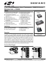
Si5351A/B/C
4 Preliminary Rev. 0.95
1. Electrical Specifications
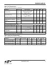
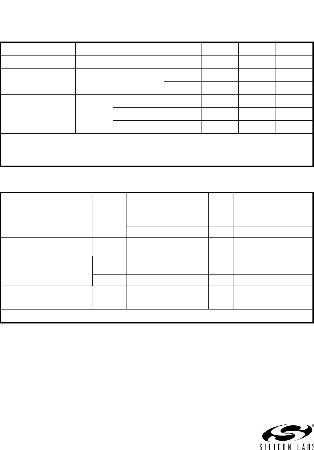
Table 1. Recommended Operating Conditions
Parameter Symbol Test Condition Min Typ Max Unit
Ambient Temperature T
A
–402585°C
Core Supply Voltage V
DD
3.0 3.3 3.60 V
2.25 2.5 2.75 V
Output Buffer Voltage V
DDOx
1.71 1.8 1.89 V
2.25 2.5 2.75 V
3.0 3.3 3.60 V
Notes:All minimum and maximum specifications are guaranteed and apply across the recommended operating conditions.
Typical values apply at nominal supply voltages and an operating temperature of 25 °C unless otherwise noted.
VDD and VDDOx can be operated at independent voltages.
Power supply sequencing for VDD and VDDOx requires that both voltage rails are powered at the same time.
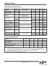
Table 2. DC Characteristics
(V
DD
= 2.5 V ±10%, or 3.3 V ±10%, T
A
= –40 to 85 °C)
Parameter Symbol Test Condition Min Typ Max Unit
Core Supply Current I
DD
Enabled 3 outputs — 22 35 mA
Enabled 8 outputs — 27 45 mA
Power Down (PDN = V
DD
)— — 20 µA
Output Buffer Supply Current
(Per Output)*
I
DDOx
C
L
=5pF — 2.2 5 mA
Input Current
I
CLKIN
CLKIN, SDA, SCL
Vin < 3.6 V
——10 µA
I
VC
VC — — 30 µA
Output Impedance Z
O
8 mA output drive current.
See "6. Design Consider-
ations" on page 21.
—85—
*Note: Output clocks less than or equal to 100 MHz.