


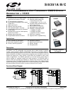
Si5351A/B/C
8 Preliminary Rev. 0.95
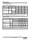
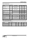
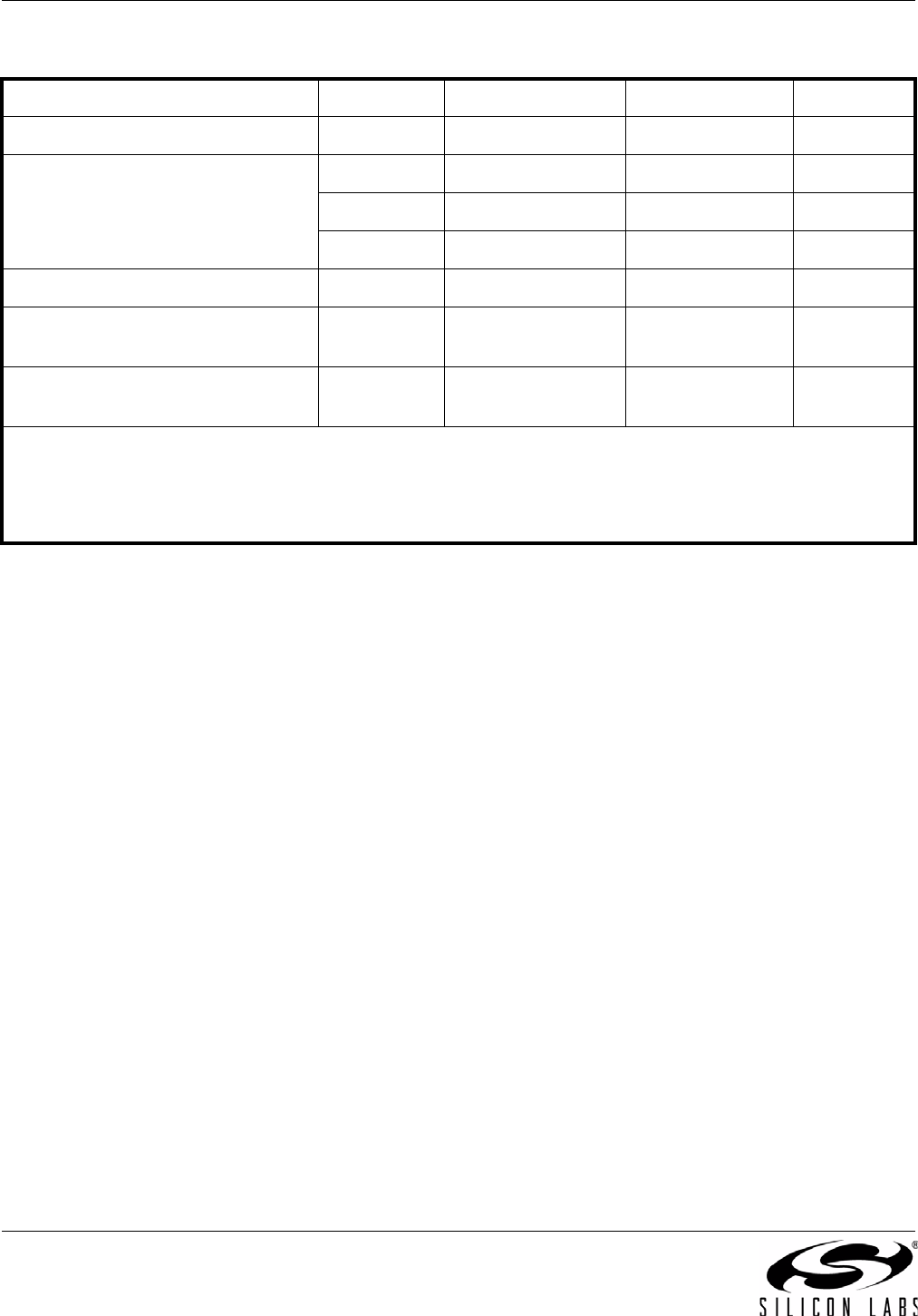
Table 9. Absolute Maximum Ratings
1
Parameter Symbol Test Condition Value Unit
DC Supply Voltage V
DD_max
–0.5 to 3.8 V
Input Voltage
V
IN_CLKIN
CLKIN, SCL, SDA –0.5 to 3.8 V
V
IN_VC
VC –0.5 to (VDD+0.3) V
V
IN_XA/B
Pins XA, XB –0.5 to 1.3 V V
Junction Temperature T
J
–55 to 150 °C
Soldering Temperature (Pb-free
profile)
2
T
PEAK
260 °C
Soldering Temperature Time at
TPEAK (Pb-free profile)
2
T
P
20–40 Sec
Notes:
1. Permanent device damage may occur if the absolute maximum ratings are exceeded. Functional operation should be
restricted to the conditions as specified in the operational sections of this data sheet. Exposure to absolute maximum
rating conditions for extended periods may affect device reliability.
2. The device is compliant with JEDEC J-STD-020.