


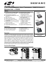
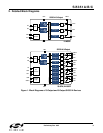
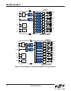
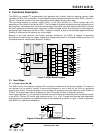

Si5351A/B/C
Preliminary Rev. 0.95 7
Table 7. I
2
C Specifications (SCL,SDA)
1
Parameter
Symbol Test Condition Standard Mode
100 kbps
Fast Mode
400 kbps
Unit
Min Max Min Max
LOW Level
Input Voltage
V
ILI2C
–0.5
0.3 x V
DDI2
C
–0.5 0.3 x V
DDI2C
2
V
HIGH Level
Input Voltage
V
IHI2C
0.7 x V
DDI2
C
3.63 0.7 x V
DDI2C
2
3.63 V
Hysteresis of
Schmitt Trigger
Inputs
V
HYS
—— 0.1 —V
LOW Level
Output Voltage
(open drain or
open collector)
at 3 mA Sink
Current
V
OLI2C
2
V
DDI2C
2
= 2.5/3.3 V 0 0.4 0 0.4 V
V
DDI2C
2
= 1.8 V — — 0 0.2 x V
DDI2C
V
Input Current I
II2C
–10 10 –10 10 µA
Capacitance for
Each I/O Pin
C
II2C
V
IN
= –0.1 to V
DDI2C
—4 — 4pF
I
2
C Bus
Timeout
T
TO
Timeout Enabled 25 35 25 35 ms
Notes:
1. Refer to NXP’s UM10204 I
2
C-bus specification and user manual, revision 03, for further details, go to:
www.nxp.com/acrobat_download/usermanuals/UM10204_3.pdf.
2. Only I
2
C pullup voltages (VDDI2C) of 2.25 to 3.63 V are supported.
Table 8. Thermal Characteristics
Parameter Symbol Test Condition Package Value Unit
Thermal Resistance
Junction to Ambient
JA
Still Air
10-MSOP 131 °C/W
24-QSOP 80 °C/W
20-QFN 51 °C/W
Thermal Resistance
Junction to Case
JC
Still Air
10-MSOP 43 °C/W
24-QSOP 31 °C/W
20-QFN 16 °C/W