AR-B7041 User¡¦s Guide
3-9
3.3.3 Battery Setting
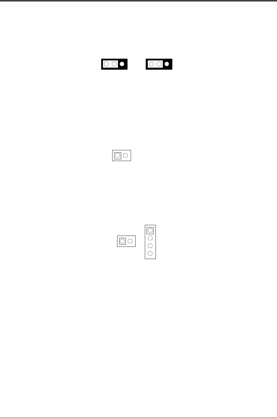
(1) Battery Charge Enable/Disable (JP2)
If the AR-B7041 uses a 3.6V Ni-Cd rechargeable battery for SRAM data retention, the on-board charge circuit can
be enabled by set the JP2 jumper. The battery will be charged when the power is on.
1 2 3
Rechargeable
Battery
1 2 3
Non-chargeable
Battery
(Factory Preset)
JP2
Figure 3-6 JP2: Battery Charge Enable/Disable
(2) Battery Output Connector (J4)
The J4 is used to connect the battery to the AR-B7017 when the AR-B7017 is going to be removed from the AR-
B7041. A two wired cable provided with the AR-B7017 is used to do this job. This would be very convenient if you
are using the SRAM on the AR-B7017 and you want to remove the AR-B7017 temporarily.
1 Battery+
2 Battery-
J4
1 2
Figure 3-7 J4: Battery Output Connector
(3) External Battery Connector (J3 & J5)
J3 and J5 allow users to connect an external 3.6 to 6 VDC battery to the AR-B7041 if the on-board battery is
empty. Only the SRAM disk will sink the battery current. If no SRAM chips are used, no battery is needed. The
battery charger on AR-B7041 does not source charge current to the external battery which connected to J3 or J5.
1 Battery+
2 Battery-
J5
4 Battery-
3 Battery+
1 2
1 Battery+
2 Battery-
J3
Figure 3-8 J3 & J5: External Battery Connector
3.4 ROM DISK INSTALLATION
The section describes the various type SSDs’ installation steps as follows. The jumper and switch adjust as SSD’ s
different type to set.
3.4.1 UV EPROM (27Cxxx)
(1) Switch and Jumper Setting
Step 1: Use jumper block to set the memory type as ROM (FLASH).
Step 2: Select the proper I/O base port, firmware address, disk drive number and EPROM type on SW1.
Step 3: Insert programmed EPROM(s) or FLASH(s) chips into sockets starting at MEM1.


