


AR-B7041 User¡¦s Guide
5-1
5. MEMORY BANKS & INDEX
5.1 USING MEMORY BANKS
This chapter provides the information about how to access the memory on the AR-B7041 without using the AR-
B7041 SSD BIOS. The AR-B7041 hardware cut every 8K bytes of memory into a memory bank. To access the
data in memory, you have to assign the chip number and the bank number. On every chip, the memory bank
number starts from the number zero. The last memory bank number depends on the size of the memory chip used
on the AR-7041. For example, if you use the 256K bytes memory chip, the bank number on every chip would be in
the range of 0 to 31. The chip number and the bank number are determined by the bank selected register and the
chip selected register on the AR-B7041.
The I/O addresses of these registers are determined by of SW1-1 and SW1-2. The memory address of the
memory bank is located on the range selected by SW1-3 and SW1-4.
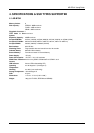
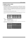
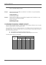
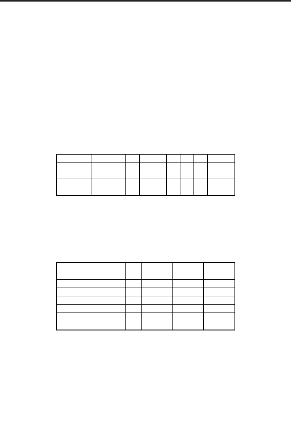
The I/O port address of the bank select register is base port+0, and the I/O port address of the chip select register
is base port +1. The following is the format of the bank select register and bank enable register.
Register I/O Port D7 D6 D5 D4 D3 D2 D1 D0
Bank Select
Register
Base + 0 WPE A6 A5 A4 A3 A2 A1 A0
Chip Select
Register
Base + 1 0 0 0 1 CS3 CS2 CS1 CS0
Where:
WPE Write protect enable bit
A6 – A0 Bank select bits, A0 is the LSB.
CS2 – CS0 Chip select bits of MEM1 to MEM8, CS0 is the LSB
CS3 0 for AR-B7041, 1 for AR-B7017
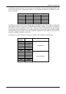
For different types of memory, A0 to A6 have different explanations. These bits are used to select the bank
number of specific memory located by CS0 to CS3.
Memory A6 A5 A4 A3 A2 A1 A0
64KB EPROM/FLASH 0 0 1 0 BS2 BS1 BS0
128KB EPROM/FLASH 0 0 1 BS3 BS2 BS1 BS0
256KB EPROM/FLASH 0 BS4 1 BS3 BS2 BS1 BS0
512KB EPROM/FLASH 0 BS4 BS5 BS3 BS2 BS1 BS0
1MB EPROM BS6 BS4 BS5 BS3 BS2 BS1 BS0
128KB SRAM 0 1 0 BS3 BS2 BS1 BS0
512KB SRAM 0 BS5 BS4 BS3 BS2 BS1 BS0