AR-B7041 User¡¦s Guide
1-1
1. OVERVIEW
This chapter provides an overview of your system features and capabilities. The following topics are covered:
l Introduction
l Packing List
l Features
1.1 INTRODUCTION
The AR-B7041 is a solid state disk card that can be used as the system disk or as a replacement for mechanical
disk drives is any IBM PC/XT/AT or compatible computer. It is ideal for, but not limited to, the following
applications:
l Diskless PC workstations
l High reliability and/or high speed access applications
l Heavy duty disk access requirements
l PC controller for industrial or line test instruments
l Environments hostile to standard floppy disks & drives (Dust, moisture, vibration, etc.)
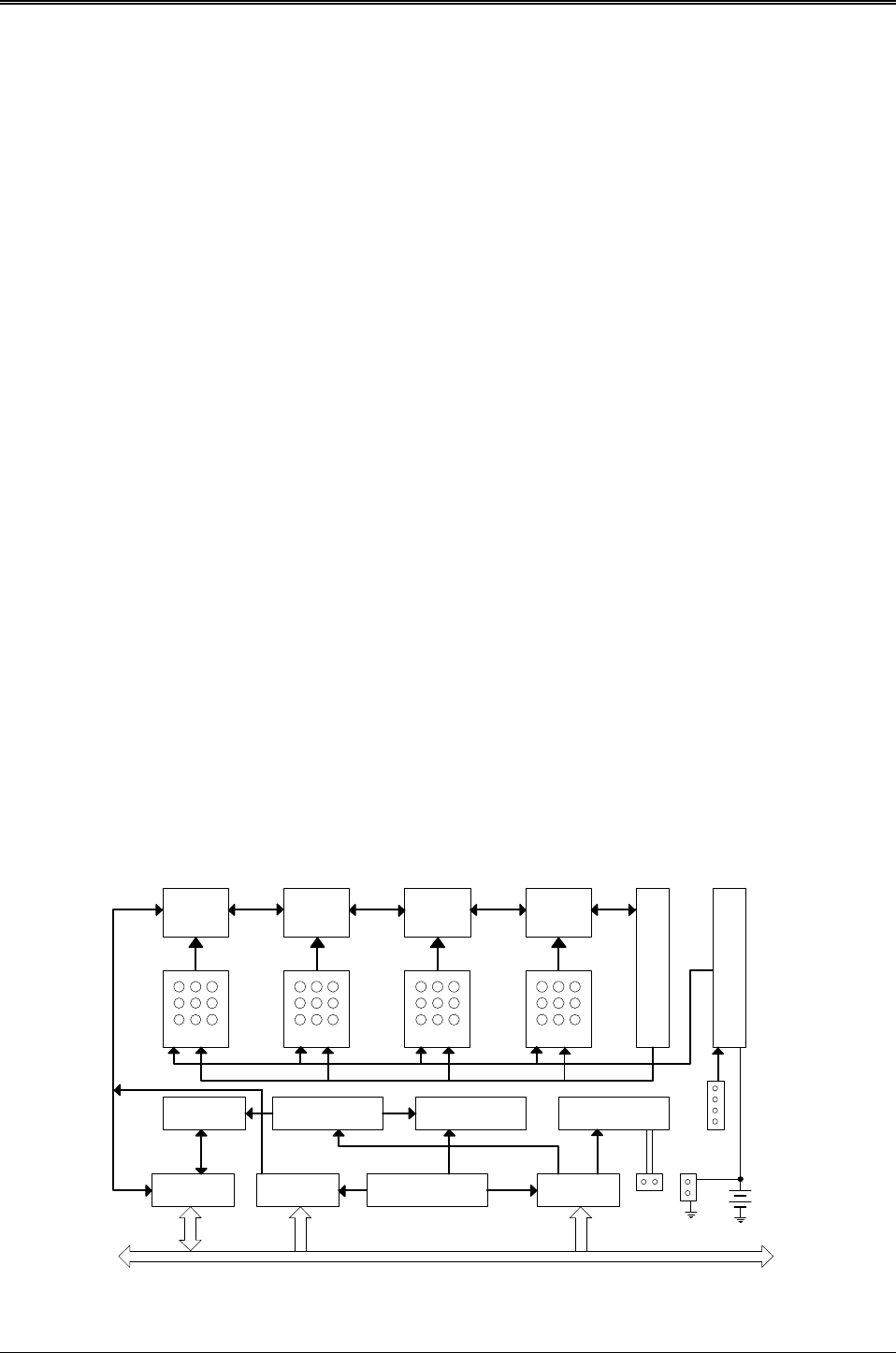
This card is a byte wide memory card that plugs into any free slot of system. Eight 32-pin JEDEC DIP sockets
may be populated with up to 8MB of EPROM, 4MB of FLASH EPROM/SRAM or combinations of them. The AR-
B7041 also provides one piggyback connector to install AR-B7017 cards (4MB ROM/RAM/FLASH module), for
maximum of 12MB disk space.
Data retention of SRAM is ensured by an on-board Lithium battery or using an external battery pack that may be
connected to the AR-B7041. A write protect function allows you to prevent data on SRAM disk or FLASH disk
from accidental deletion or overwrite.
The AR-B7041 and AR-B7017 supports 5V FLASH EPROMs. This enables you to program FLASH EPROMs on-
board directly. If small page (less or equal to 512 bytes per page) 5V FLASHs are used, you can format FLASH
disk and copy files onto the FLASH disk just like using a normal disk. This feature will extend the life of your
FLASH EPROM chips by only reprogram a small area. You should use all of the related DOS command (such as
COPY, DEL, …etc.) to update files on the 5V FLASH disk.
The AR-B7041 ROM/RAM disk card is extremely easy to install and use. However, it is advised that you read this
manual before you begin to install.
M1 M2 M3 M4
MEM1
MEM2
MEM3
MEM4
MEM5
MEM6
MEM7
MEM8
ROM DISK
BIOS
I/O BUFFER
AND LATCH
FLASH EPROM
VPP GENERATOR
WATCHDOG TIMER
ADDRESS AND
DATA BUFFER
MEMORY
DECODER
I/O DECODER
SW1
CN1
1 2 3 4 5 6 7 8 9 10
J1
J4
J5
BAT1
ISA BUS
Figure 1-1 AR-B7041 Functional Block Diagram


