


1-4
X7DBT/X7DBT-INF/X7DGT/X7DGT-INF User's Manual
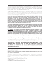
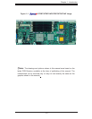
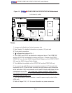
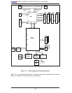
Figure 1-2. X7DBT/X7DBT-INF/X7DGT/X7DGT-INF Motherboard
1. Jumpers not indicated are for test purposes only.
2. See Chapter 2 for detailed information on jumpers, I/O ports and
JF1 front panel connections.
3. " " indicates the location of Pin 1.
4. The X7DBT and X7DGT are identical in design and layout. The X7DBT-INF
and the X7DGT-INF are identical in design and layout. However, the X7DBT/
X7DBT-INF uses the Intel 5000P chipset (North Bridge), and the X7DGT/X7DGT-
INF uses the 5000X chipset (North Bridge).
5. The Infi niBand is available on the X7DGT-INF and the X7DBT-INF only.
6. You cannot use both 20-pin power connectors located at J17 (the right side
connector) and JP10 (the left side connector) as input power supply connectors
at the same time. Only one connector can be used for input power supply to the
motherboard at one time. *For proper use of these proprietary PWR Connec-
tors, please customize your PWR cables based on the Power Connector Pin-Out
Defi nitions listed on Page 2-14.
7. The 4-pin Auxiliary Power Connector is used for power supply output to the
HDDs only.
8. Refer to Pages 2-14, 2-15 for more information on power connectors.
(not drawn to scale)
*Notes:
S
UPER X7DBT
LAN1
®
LAN2
Fan1/2
FP CTRL
SMB
Battery
N
orth
Bridge
VGA
Infini-
USB0/1
JPG1
South
Bridge
DIMM 1A
(Bank 1)
JPL2
PCI-E x8
D
IMM 1B (Bank
1
)
D
IMM 2A (Bank
2)
DIMM 2B
(
Bank 2)
DIMM 3
A (
Bank 3)
D
IMM 3B (Bank
3)
D
IMM 4A (Bank
4)
DIMM 4B (Ban
k 4)
JBT1
JWOR
JWOL
J
29
LAN
CTRL
J
USB1
SIMS0
LE3
COM2
J
PL1
J
PCE1
SATA3
JI
2
C1
JI
2
C2
J7
JP1
JOH1
J
18
JVGA1
J
L1
4-Pin
P
WR
BIOS
Buzzer
SP1
USB2/3
JUSB2
CPU1
JF1
Fan3/4
Fan5/6
LE1
VGA
CTRL
S I/O
LE
2
JCOM2
Band
I
NF
Ctrl
Video
Memory
J7B1
J7B2
J7
B
3
J8B1
J8B2
J8B3
J9B1
J9B2
J1
SATA2
SATA0
SATA1
CPU2
Fan7/8
20-Pin P
WR
20-PinPWR
J17
JP10
SGPI
O
WD