


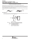
TNETX3270
ThunderSWITCH 24/3 ETHERNET SWITCH
WITH 24 10-MBIT/S PORTS AND 3 10-/100-MBIT/S PORTS
SPWS043B – NOVEMBER 1997 – REVISED APRIL 1999
56
POST OFFICE BOX 655303 • DALLAS, TEXAS 75265
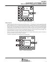
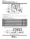
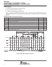
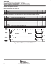
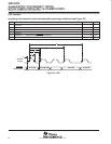
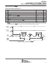
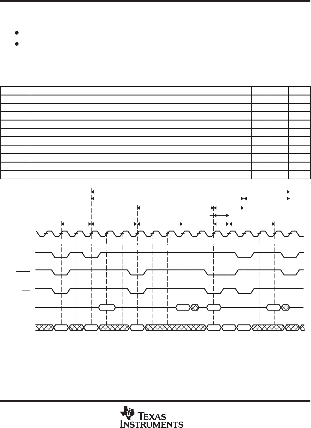
SDRAM interface
The SDRAM interface observes two types of timing:
Multicycle timings between commands
Subcycle timings between signals and DCLK
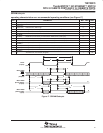
Figure 16 illustrates the SDRAM interfaces signal timing in which each type of SDRAM command and its
interrelated timings are shown. It is not intended to be representative of any particular receive or transmit buffer
operation.
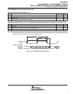
SDRAM command to command (see Figure 16)
SYMBOL PARAMETER MIN MAX UNIT
t
RSA
MRS to ACTV or REFR 24 ns
t
RC
Row cycle time (ACTV to REFR to next ACTV or REFR) 120 ns
t
RAS
Row active time (ACTV to DCAB) 72 ns
t
RP
Row recharge time (DCAB to ACTV, REFR, or MRS) 36 ns
t
RCD
Row to column delay (ACTV to READ or WRT) 36 ns
t
AC3
Column access time [READ (CAS) latency] (READ to data sample) 36 ns
n
CCD
Column address to column address (WRT to next READ or WRT, or READ to next READ) 24 ns
n
CWL
Last data or write to new column address (WRT to next READ or WRT) 24 ns
t
RWD
Read to write delay (READ to next WRT) 60 ns
t
WR
Write recovery time (WRT to DCAB) 24 ns
DCLK
t
RC
t
RP
t
RWD
t
WR
n
CWL
n
CCD
t
RCD
t
RAS
t
RSA
t
AC3
t
AC3
DRAS
DCAS
DW
DD31–DD00
DA13–DA00
REGISTER
SETTINGS
BUFFOP READ1 WRITE
READ2
MODE ROW READ1 WRITE READ2 XXXX
DA10=0 DA10=0 DA10=1DA10=0
NOOP NOOP
ACTV
READ READ
DCAB
REFRNOOP
NOOP NOOP
NOOP
NOOP
NOOP
WRT
NOOP
NOOPMRS
Figure 16. SDRAM Command to Command