


TNETX3270
ThunderSWITCH 24/3 ETHERNET SWITCH
WITH 24 10-MBIT/S PORTS AND 3 10-/100-MBIT/S PORTS
SPWS043B – NOVEMBER 1997 – REVISED APRIL 1999
58
POST OFFICE BOX 655303 • DALLAS, TEXAS 75265
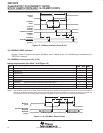
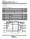
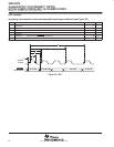
DIO/DMA interface
The DIO interface is asynchronous to allow easy adaptation to a range of microprocessor devices and computer
system interfaces.
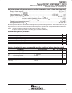
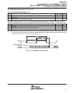
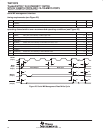
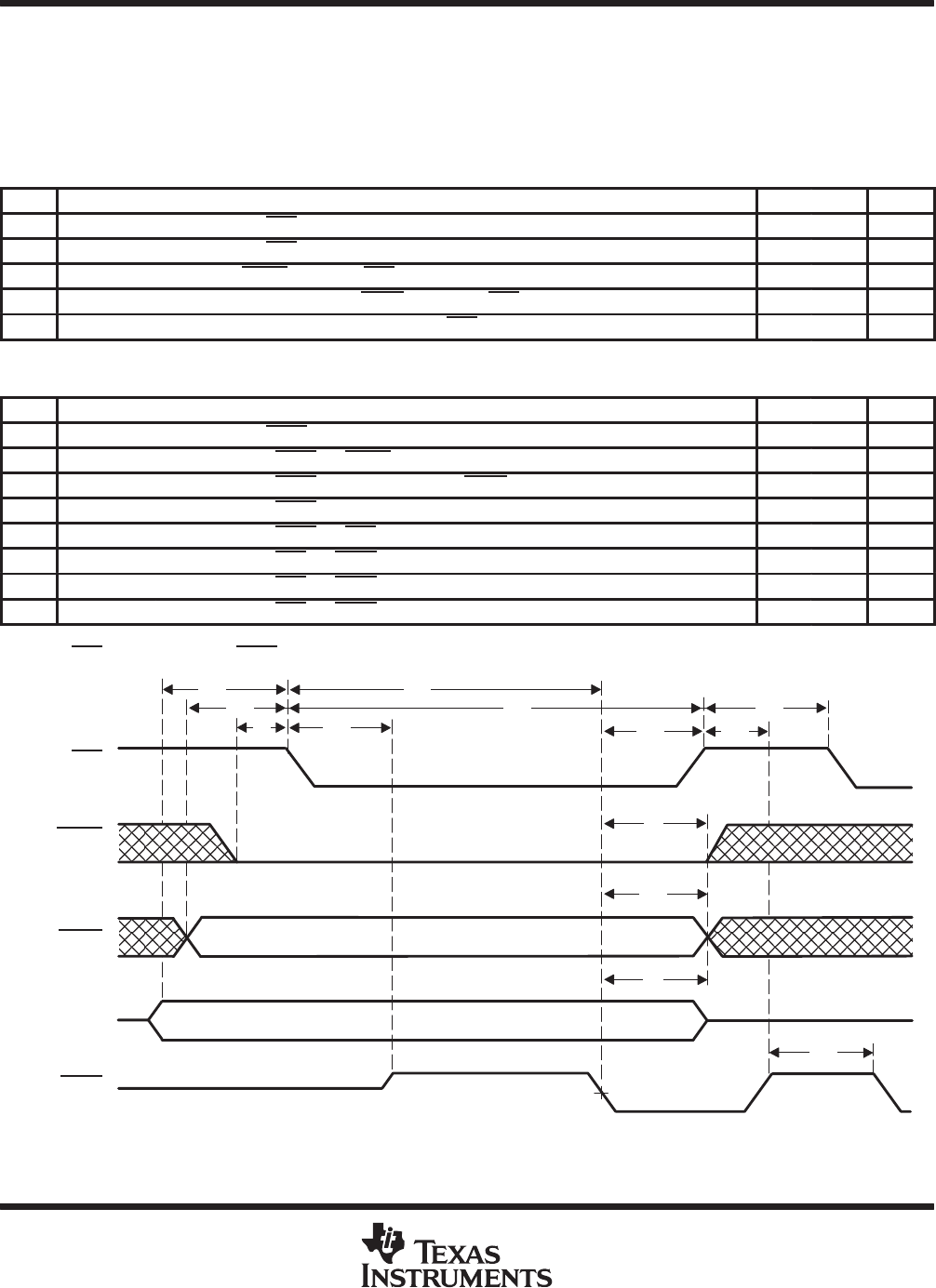
DIO/DMA write cycle
timing requirements (see Figure 18)
NO. MIN MAX UNIT
1 t
w(SCSL)
Pulse duration, SCS low 24 ns
2 t
w(SCSH)
Pulse duration, SCS high 12 ns
3 t
su(SRNW)
Setup time, SRNW low before SCS↓ 0 ns
4 t
su(SAD)
Setup time, SAD1–SAD0 and SDMA valid before SCS↓ 0 ns
5 t
su(SDATA)
Setup time, SDATA7–SDATA0 valid before SCS↓ 0 ns
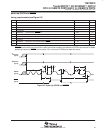
operating characteristics over recommended operating conditions (see Figure 18)
NO. PARAMETER MIN MAX UNIT
6 t
w(SRDYH)
Pulse duration, SRDY high 12 ns
7 t
d(SRNW)
Delay time, from SRDY↓ to SRNW↑ 0 ns
8 t
d(SAD)
Delay time, from SRDY↓ to SAD1–SAD0 and SDMA invalid 0 ns
9 t
d(SDATA)
Delay time, from SRDY↓ to SDATA7–SDATA0 invalid 0 ns
10 t
d(SCS)
Delay time, from SRDY↓ to SCS↑ 0 ns
11 t
d(SRDY)1
Delay time, from SCS↓ to SRDY↑ 0 ns
12 t
d(SRDY)2
Delay time, from SCS↓ to SRDY↓
†
0 ns
13 t
d(SRDY)3
Delay time, from SCS↑ to SRDY↑ 0 24 ns
†
When the switch is performing certain internal operations (e.g., EEPROM load), there may be a considerable delay (approximately 25–100 ms)
between SCS
being asserted and SRDY being asserted.
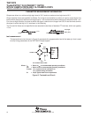
Z
SRNW
(input)
SCS
(input)
12
1
4
5
3
11
10
8
7
9
6
13
SAD1–SAD0,
SDMA
(inputs)
SDATA7–
SDATA0
(inputs)
SRDY
(output)
2
Z
Z
Figure 18. DIO/DMA Write Cycle