


TNETX3270
ThunderSWITCH 24/3 ETHERNET SWITCH
WITH 24 10-MBIT/S PORTS AND 3 10-/100-MBIT/S PORTS
SPWS043B – NOVEMBER 1997 – REVISED APRIL 1999
57
POST OFFICE BOX 655303 • DALLAS, TEXAS 75265
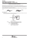
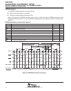
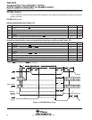
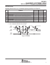
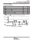
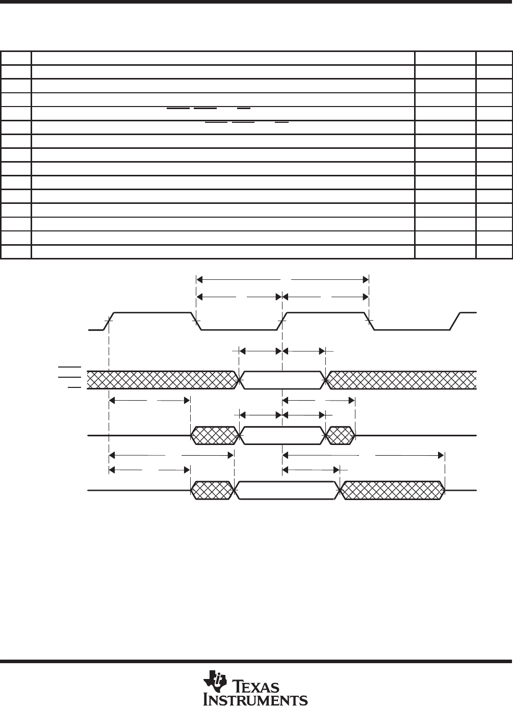
SDRAM subcycle
operating characteristics over recommended operating conditions (see Figure 17)
NO.
PARAMETER MIN MAX UNIT
1 t
c(DCLK)
Cycle time, DCLK 12 12 ns
2 t
w(DCLKL)
Pulse duration, DCLK low 5 ns
3 t
w(DCLKH)
Pulse duration, DCLK high 5 ns
4 t
d(DCLK)
Delay time, from DA, DRAS, DCAS, and DW valid to DCLK↑ 4 ns
5 t
d(DA)
Delay time, from DCLK↑ to DA, DRAS, DCAS, and DW invalid 2 ns
6 t
en(DDW)
Enable time, from DCLK↑ to before DD31–DD00 driven (write cycle) 0 ns
7 t
en(DDR)
Enable time, from DCLK↑ to before DD31–DD00 driven (read cycle) 0 ns
8 t
dis(DDW)
Disable time, from DCLK↑ to after DD31–DD00 (after final write cycle) to Z state 10 ns
9 t
dis(DDR)
Disable time, from DCLK↑ to after DD31–DD00 (after final read cycle) to Z state 11 ns
10 t
d(DDW)1
Delay time, from DD valid to DCLK↑ (write cycle) 4 ns
11 t
d(DDW)2
Delay time, from DCLK↑ to DD31–DD00 Z state (write cycle) 2 ns
12 t
d(DDR)1
Delay time, from DCLK↑ to DD31–DD00 valid (read cycle) 10 ns
13 t
d(DDR)2
Delay time, from DCLK↑ to DD31–DD00 invalid (read cycle) 0 ns
t
t
Transition time, rise and fall, all signals 1 4 ns
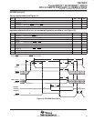
DCLK
(output)
1
DA13–DA00
DRAS
DCAS
DW
(outputs)
DD31–DD00
(during writes)
(output)
DD31–DD00
(during reads)
(input)
Z
Z
Z
Z
2 3
4 5
6
10
8
11
12 9
137
Figure 17. SDRAM Subcycle