


AR-B1375/AR-B1376 User s Guide
9-1
9. USING MEMORY BANKS
This appendix provides the information about how to access the memory on the AR-B1375 and AR-B1376 without
using the AR-B1375 and AR-B1376 SSD BIOS. The AR-B1375 and AR-B1376 hardware divides every 8K bytes of
memory into a memory bank. To access the data in the memory, you have to assign the chip number and the bank
number. On every chip, the memory bank number starts from zero. The last memory bank number depends on the
size of the memory chip used on the AR-B1375 and AR-B1376. For example, if you use the 256K bytes memory
chip, the bank number on every chip would be in the range of 0 to 31. The chip numbers and the bank numbers
are determined by the bank select register on the AR-B1375 and AR-B1376.
The I/O address of these registers are determined by SW1-1. The memory address of the memory bank is located
on the range selected by SW1-2.
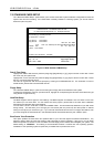
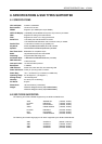
The I/O port address of the bank select register is base port+0, and the I/O port address of the chip select register
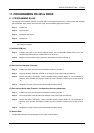
is base port +2. The following is the format of the bank select register and bank enable register.
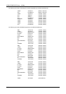
Register I/O Port D7 D6 D5 D4 D3 D2 D1 D0
Bank Select Register Base +0 WPE A6 A5 A4 A3 A2 A1 A0
Chip Select Register Base +2 0 0 0 1 CS1 CS0 X X
Where:
WPE Write protect enable bit
A6~A0 Bank select bits, A0 is the LSB
CS1~CS0 Chip select bits of MEM1 to MEM3
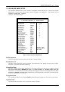
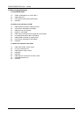
Where:
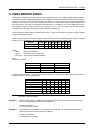
CS1-CS0 : Chip select
CS1 CS0 Socket
0 0 Disable
0 1 MEM1
1 0 MEM2
1 1 MEM3
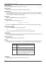
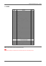
For different types of memory, A0 to A6 have different explanations. These bits are used to select the bank number
of specific memory located in CS0 and CS1.
Memory A6 A5 A4 A3 A2 A1 A0
64KB EPROM (FLASH) 0 0 1 0 BS2 BS1 BS0
128KB EPROM (FLASH) 0 0 0 BS3 BS2 BS1 BS0
256KB EPROM (FLASH) 0 BS4 1 BS3 BS2 BS1 BS0
512KB EPROM (FLASH) 0 BS4 BS5 BS3 BS2 BS1 BS0
1MB EPROM (FLASH) BS6 BS4 BS5 BS3 BS2 BS1 BS0
128KB SRAM 0 1 0 BS3 BS2 BS1 BS0
512KB SRAM 0 BS5 BS4 BS3 BS2 BS1 BS0
NOTE : BS0 to BS5 are the memory bank select bits. For example, 128KB memory has sixteen 8K-byte banks, so
4 bits (BS0 to BS3) are needed.
Example 1:
Select the 10th bank of the MEM1 on the AR-B1375 and AR-B1376. The AR-B1375 and AR-B1376
is using 27C020 (256K*8), and the base port is &H210.
100 base_port=&H210
110 OUT base_port+0,&H59
Example 2:
Select the 40th bank of MEM3 on the AR-B1375 and AR-B1376. The AR-B1375 and AR-B1376 is
using 27C040 (512K*8), and the base port is &H390.
200 base_port=&H290
210 OUT base_port+0,&HD7