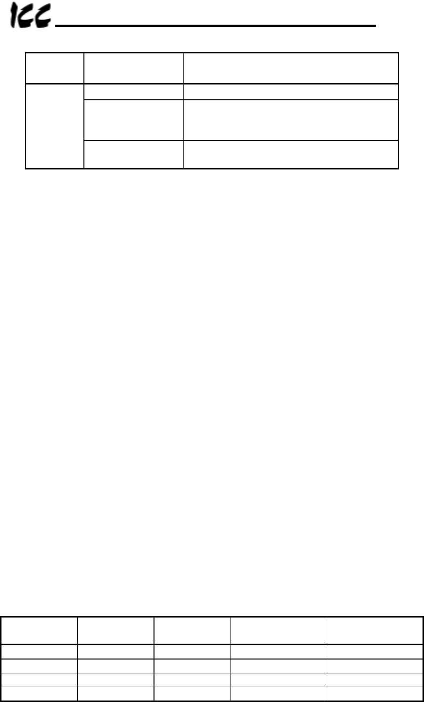
14
Holding
Register
Write Data Meaning
0x5A5A Reset the MDB-100
0xFEBA
Reset the MDB-100 and return MDB-100
configuration registers to factory default
values.
0x6111
Any other value
Return “ILLEGAL DATA VALUE”
exception
NOTE 1:
Throughout this document, hexadecimal (base 16) numbers will be
represented by a preceding “0x” or by a trailing “H” designator, decimal
(base 10) numbers will be represented by a trailing subscripted “10”
designator, and binary (base 2) numbers will be represented by a trailing
“B” designator. Binary numbers will always be written with their most
significant bit (MSB) at the left, and their least significant bit (LSB) to the
right (next to the “B”).
For example, 0x6111 = 6111H = 24849
10
= 0110 0001 0001 0001B.
NOTE 2:
The Modbus specification lists two addresses for each holding register (4X
reference) and coil (0X reference). These are referred to as the
“addressed as” and “known” as values. In all instances, registers and
coils are addressed starting at zero; i.e. register 1 is addressed as 0, and
coil 15 is addressed as 14, etc. Throughout this document, all addresses
given for coils and holding registers will be their “addressed as” values
unless otherwise specified. In other words, add 1 to the register/coil
address given to obtain its “known as” value. For example, the S7 drive’s
inverter number parameter is 0802H (= 0x0802 = 2050
10
.) Therefore, this
register would be “known as” 2051. Refer to the Modbus Protocol
Reference Guide for a more detailed explanation of this issue.
The station address set via switch SW2 must be set using binary encoding. In this
case, SW2 #1 represents bit #0 of the address, and SW2 #8 represents bit #7.
When one of the DIP switches of SW2 is turned ON, the corresponding address bit is
1, and when one of the switches is turned OFF, the corresponding address bit is 0.
For example, if an address of 169
10
is desired, the conversion calculation would be
performed as follows:
169
10
= 0xA9 = 1010 1001B, therefore switches SW2 #1, #4, #6 and #8 should be
ON, and #2, #3, #5 and #7 should be OFF.
Some more address configuration examples (factory default setting = 1):
Address
(Decimal)
Address
(Hex)
Address
(Binary)
“ON”
Switches
“OFF”
Switches
1 (min) 0x01 0000 0001B #1
#2 ∼ #8
63 0x3F 0011 1111B
#1 ∼ #6
#7, #8
200 0xC8 1100 1000B #4, #7, #8
#1 ∼ #3, #5, #6
247 (max) 0xF7 1111 0111B
#1 ∼ #3, #5 ∼ #8
#4


