


19
10. Modbus Programming Interface
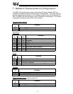
10.1 Overview
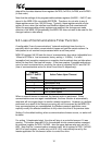
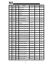
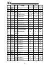
Three types of Modbus data may be accessed via the MDB-100. These are holding
registers (4x reference), read-only coils (0x reference) and write-only coils (0x
reference). In order to access 2 drives within the allocated holding register map
(0x0000 ∼ 0xFFFF), each drive is assigned one half of the register space.
Drive A occupies the area from register 0x0000 to 0x7FFF. This area also contains
several network and drive configuration registers (such as the programmable pointer
and data registers, network timeout registers, etc.) that reside within the MDB-100
only. The registers which the MDB-100 uses for these functions are not accessible in
the drive. Currently, these registers are unoccupied in the drive, and therefore no
loss of access to any drive parameters exists. Most of the registers for drive A are
mapped to the exact same “communication number” that they are allocated in the S7
drive by Toshiba. Refer to the VF-S7 Serial Communications Option Manual for a list
of communication numbers. The only exception to this direct mapping are the
registers that occupy communication numbers larger than 0x8000. For these
parameters, their corresponding Modbus holding registers can be obtained by setting
the MSB (bit #15) of their communication number to 0.
For example, the communication number for drive A’s bus voltage parameter is
0xFE04 (1111 1110 0000 0100B). Setting bit #15 to 0, we obtain the binary value
0111 1110 0000 0100B, or 0x7E04. Reading from Modbus holding register 0x7E04
(“known as” 0x7E05), therefore, will return the bus voltage from drive A.
Drive B occupies the area from register 0x8000 to 0xFFFF. This area also contains
the MDB-100 –specific drive configuration registers that correspond to those
available for drive A. Most of the registers for drive B are not mapped to the exact
same “communication number” that they are allocated in the S7 drive by Toshiba.
For these parameters, their corresponding Modbus holding registers can be obtained
by setting the MSB (bit #15) of their communication number to 1.
For example, the communication number for drive B’s deceleration time #1
parameter is 0x0010 (0000 0000 0001 0000B). Setting bit #15 to 1, we obtain the
binary value 1000 0000 0001 0000B, or 0x8010. Writing to Modbus holding register
0x8010 (“known as” 0x8011), therefore, will modify the deceleration time #1
parameter for drive B.
The only exception to this mapping modification requirement for drive B are the
registers that occupy communication numbers larger than 0x8000. For these
parameters, the communication numbers given in the VF-S7 Serial Communications
Option Manual correspond exactly to their assigned “addressed as” holding registers
(for example, holding register 0xFE10 will access the past trip #1 value from drive B).
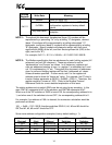
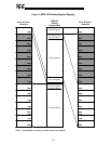
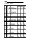
Refer to Figure 2 on page 20 for a graphical representation of the holding register
mapping that exists in the MDB-100 Modbus interface.