


DS8100A
2
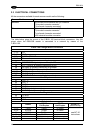
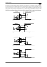
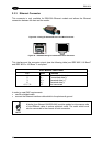
The OUT3 electrical features are given below:
Maximum voltage ± 100 V
Collector current (pulse) 240 mA Max.
Collector current (continuous) 150 mA Max.
R on 6 – 15 Ω
R off > 500 Ω
Off-state leakage current < 1 µA
Maximum power dissipation 550 mW at 50°C (Ambient temperature).
DS8100A
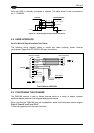
USER INTERFACE
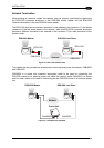
Vext
100 Vdc max
A/B
B/A
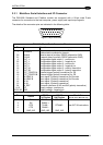
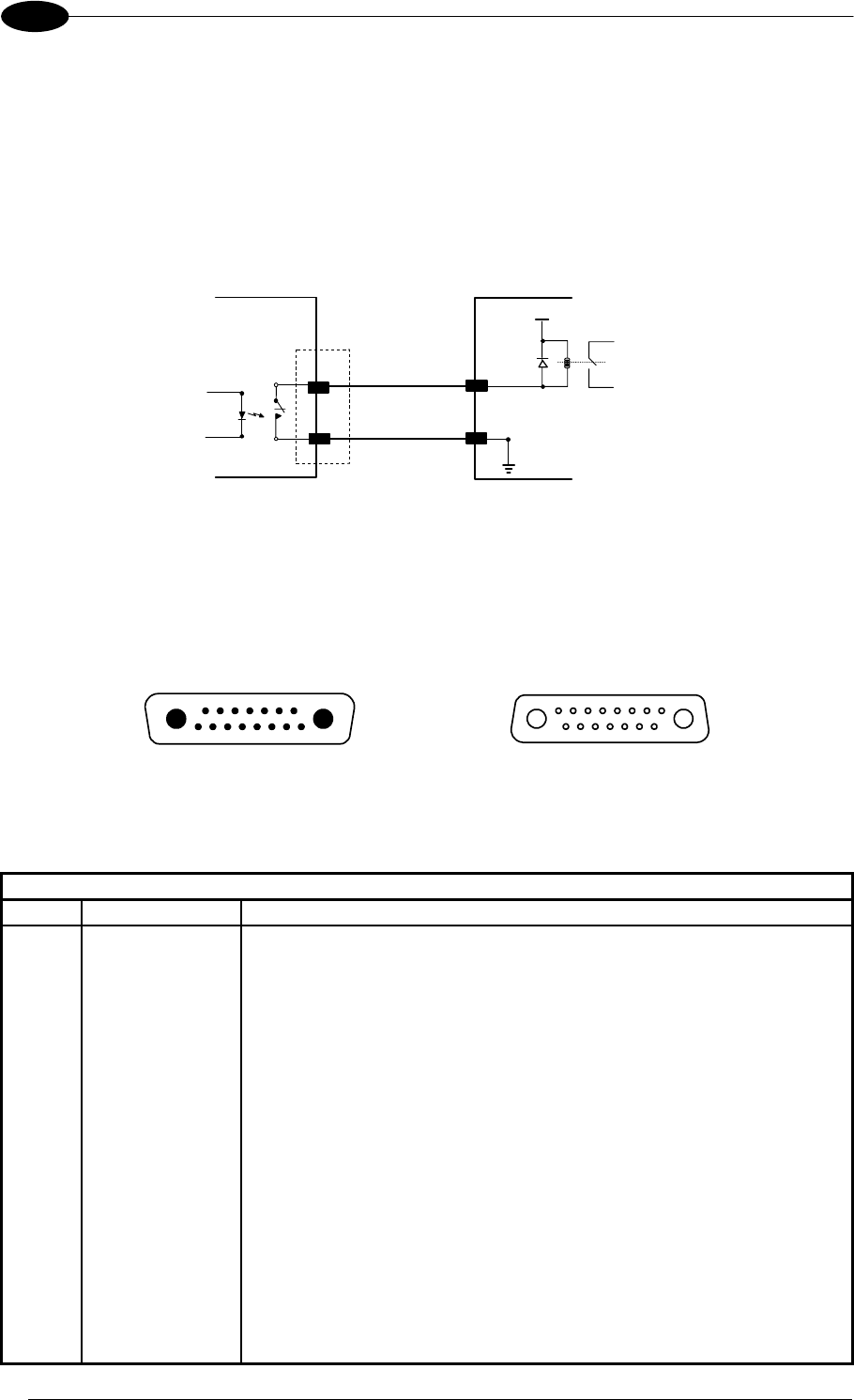
Figure 21 – Output 3 Interface
The command signal is filtered and generates a delay of about 50 µs for OUT1 and OUT2
and 1 ms for OUT3.
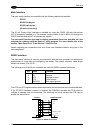
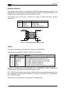
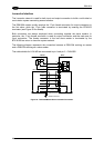
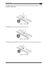
2.3.2 Lonworks Input/Output Connector
A1
A2
1
15
scanner side
external view
A1
A2
1
15
OUTPUT (female)
INPUT (male)
Figure 22 - Lonworks INPUT/OUTPUT Connectors
The following pinout is valid for the INPUT connector as well as for the OUTPUT connector.
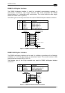
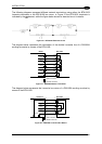
Lonworks INPUT/OUTPUT 17-pin Connector Pinout
Pin Name Function
A1 GND supply voltage (negative pin)
A2 VS supply voltage 20 to 30 vdc (positive pin)
1 CHASSIS Cable shield A – internally connected by capacitor to chassis
2 n.c. Not connected
3 CHASSIS Cable shield B – internally connected by capacitor to chassis
4 n.c. Not connected
5 n.c. Not connected
6 n.c. Not connected
7 VS_I/O Supply voltage of I/O circuit
8 Lon A+ Lonworks a line (positive pin)
9 Lon A- Lonworks a line (negative pin)
10 Lon B+ Lonworks b line (positive pin)
11 Lon B- Lonworks b line (negative pin)
12 SYS_I/O System signal
13 SYS_ENC_I/O System signal
14 Reserved Internally connected
15 Ref_I/O Reference voltage of I/O circuit
18