


2-2
MPC860T (Rev. D) Fast Ethernet Controller Supplement
MOTOROLA
PRELIMINARYÑSUBJECT TO CHANGE WITHOUT NOTICE
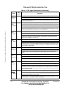
PD[12]
L1RSYNCB
MII_MDC
R16 General-purpose I/O port D bit 12ÑThis is bit 12 of the general-purpose I/O port D.
L1RSYNCBÑInput receive data sync signal to the TDM channel B.
MII management data clockÑOutput clock provides a timing reference to the PHY for data
transfers on the MDIO signal.
PD[11]
RXD3
MII_TX_ER
T16 General-purpose I/O port D bit 11ÑThis is bit 11 of the general-purpose I/O port D.
RXD3ÑReceive data for serial channel 3.
MII transmit errorÑOutput signal when asserted for one or more clock cycles while TX_EN is
asserted shall cause the PHY to transmit one or more illegal symbols. Asserting TX_ER has
no effect when operating at 10 Mbps or when TX_EN is negated.
PD[10]
TXD3
MII_RXD[0]
W18 General-purpose I/O port D bit 10ÑThis is bit 10 of the general-purpose I/O port D.
TXD3ÑTransmit data for serial channel 3.
MII receive data 0ÑInput signal RXD[0] represents bit 0 of the nibble of data to be
transferred from the PHY to the MAC when RX_DV is asserted. In 10 Mbps serial mode,
RXD[0] is used and RXD[1Ð3] are ignored.
PD[9]
RXD4
MII_TXD[0]
V17 General-purpose I/O port D bit 9ÑThis is bit 9 of the general-purpose I/O port D.
RXD4ÑReceive data for serial channel 4.
MII transmit data 0ÑOutput signal TXD[0] represents bit 0 of the nibble of data when TX_EN
is asserted and has no meaning when TX_EN is negated. In 10Mbps serial mode, TXD[0] is
used and TXD[1Ð3] are ignored.
PD[8]
TXD4
MII_RX_CLK
W17 General-purpose I/O port D bit 8ÑThis is bit 8 of the general-purpose I/O port D.
TXD4ÑTransmit data for serial channel 4.
MII receive clockÑInput clock which provides a timing reference for RX_DV, RXD, and
RX_ER.
PD[7]
RTS3
MII_RX_ER
T15 General-purpose I/O port D bit 7ÑThis is bit 7 of the general-purpose I/O port D.
RTS3ÑActive-low request to send output indicates that SCC3 is ready to transmit data.
MII receive errorÑWhen Input signal RX_ER and RX_DV are asserted, the PHY has
detected an error in the current frame. When RX_DV is not asserted, RX_ER has no effect.
PD[6]
RTS4
MII_RX_DV
V16 General-purpose I/O port D bit 6ÑThis is bit 6 of the general-purpose I/O port D.
RTS4ÑActive low request to send output indicates that SCC4 is ready to transmit data.
MII receive data validÑWhen input signal RX_DV is asserted, the PHY is indicating that a
valid nibble is present on the MII. This signal shall remain asserted from the Þrst recovered
nibble of the frame through the last nibble. Assertion of RX_DV must start no later than the
SFD and exclude any EOF.
PD[5]
REJECT2
MII_TXD[3]
U15 General-purpose I/O port D bit 5ÑThis is bit 5 of the general-purpose I/O port D.
Reject 2ÑThis input to SCC2 allows a CAM to reject the current Ethernet frame after it
determines the frame address did not match.
MII transmit data 3ÑOutput signal TXD[3] represents bit 3 of the nibble of data when TX_EN
is asserted and has no meaning when TX_EN is negated.
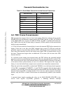
Table 2-1. FEC Signal Descriptions (Continued)
Name
Pin
Number
Description
Fr
eescale S
emiconduct
or
, I
Freescale Semiconductor, Inc.
For More Information On This Product,
Go to: www.freescale.com
nc...