


MOTOROLA Chapter 6. Programming Model 6-15
PRELIMINARYÑSUBJECT TO CHANGE WITHOUT NOTICE
be non-zero to source a read or write management frame. After the management frame is
complete, MII_SPEED may optionally cleared to turn off the MDC. The MDC generated
has a 50% duty cycle except when MII_SPEED is changed during operation (changes take
effect following either a rising or falling edge of MDC).
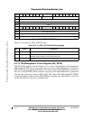
If the system clock is 25 MHz, programming this register to 0x0000_000A generates an
MDC frequency of 25 MHz * 1/10 = 2.5 MHz.
Table 6-16 shows optimum values for MII_SPEED as a function of system clock frequency.
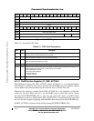
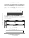
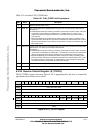
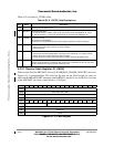
6.2.15 FIFO Receive Bound Register (R_BOUND)
The R_BOUND register, Figure 6-15, is a read-only register the user can read to determine
the upper address bound of the FIFO RAM. Drivers can use this value, along with the
R_FSTART and X_FSTART to appropriately divide the available FIFO RAM between the
transmit and receive data paths.
Table 6-17 describes R_BOUND Þelds.
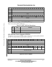
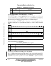
Table 6-16. Programming Examples for MII_SPEED Register
System Clock Frequency MII_SPEED[MII_SPEED] MDC frequency
25 MHz 0x05 2.5 MHz
33 MHz 0x07 2.36 MHz
40 MHz 0x08 2.5 MHz
50 MHz 0x0A 2.5 MHz
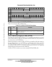
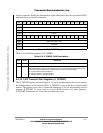
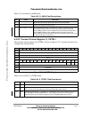
Bits 0 1 2 3 4 5 6 7 8 9 10 11 12 13 14 15
Field Ñ
Reset 0000_0000_0000_0000
R/W Read only
Addr 0xECC
Bits 16 17 18 19 20 21 22 23 24 25 26 27 28 29 30 31
Field Ñ 1 R_BOUND Ñ
Reset 0000_0100_0000_0000
R/W Read only
Addr 0xECE
Figure 6-15. R_BOUND Register
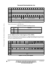
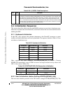
Table 6-17. R_BOUND Field Descriptions
Bits Name Description
0Ð21 Ñ Reserved. Note all bits read back as 0 except for 21 which returns a 1.
Fr
eescale S
emiconduct
or
, I
Freescale Semiconductor, Inc.
For More Information On This Product,
Go to: www.freescale.com
nc...