


MOTOROLA Chapter 4. Parallel I/O Ports 4-1
PRELIMINARYÑSUBJECT TO CHANGE WITHOUT NOTICE
Chapter 4
Parallel I/O Ports
40
40
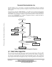
This chapter shows how to use port D pin multiplexing to support Fast Ethernet controller
(FEC) operations.
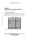
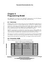
4.1 Port D Pin Functions
Each of the 13 port D pins is independently conÞgured as a general-purpose I/O pin if the
corresponding port D pin assignment register (PDPAR) bit is cleared. Each pin is
conÞgured as a dedicated on-chip peripheral pin if the corresponding PDPAR bit is set.
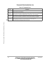
Refer to Table 4-1 for the default description of all port D pin options.
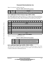
When the port pin is conÞgured as a general-purpose I/O pin, the signal direction for that
pin is determined by the corresponding control bit in the port D data direction register
(PDDIR). The port I/O pin is conÞgured as an input if the corresponding PDDIR bit is
cleared; it is conÞgured as an output if the corresponding PDDIR bit is set. All PDPAR bits
and PDDIR pins are cleared on total system reset, conÞguring all port D pins as general-
purpose input pins.
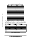
PD[13:8] peripheral functions (RXD3, TXD3, RXD4, TXD4) are alternately available on
PA[11:8]. PD[7:5], and PD12 peripheral functions (R
TS3, RTS4, and L1RSYNCB) are
alternately available on PC[13:12] and PC6. Functions REJECT3
and REJECT4 are lost
when MII mode is used. The peripheral functions L1TSYNCB, L1TSYANCA and
L1RSYNCA found on PD[15:13] are alternatively available on PC7, PC5, and PC4.
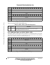
Note: The reserved bits of the PDPAR must be written with zeros. Failure to do so may
result in one or more of the following:
¥ No events on SCC3 and SCC4.
¥ No events on any CPM peripheral.
¥ Pin multiplexing of Port D will not be as expected
Fr
eescale S
emiconduct
or
, I
Freescale Semiconductor, Inc.
For More Information On This Product,
Go to: www.freescale.com
nc...