


MOTOROLA Chapter 6. Programming Model 6-19
PRELIMINARYÑSUBJECT TO CHANGE WITHOUT NOTICE
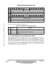
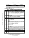
Table 6-21 describes FUN_CODE Þelds.
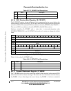
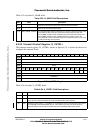
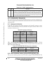
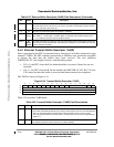
6.2.20 Receive Control Register (R_CNTRL)
The R_CNTRL register, shown in Figure 6-20, is programmed by the user to control the
operational mode of the receive block.
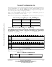
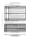
Table 6-21. FUN_CODE Field Descriptions
Bits Name Description
0 Ñ Reserved. This bit reads as zero.
1Ð2 DATA_BO Byte order. Supplied to the SDMA interface during receive and transmit data DMA transfers.
00 Reserved
01 PowerPC little-endian byte ordering. Considering each double word in the buffer, data bytes
is received to or transmitted from address 0b111 to 0b000. This is to conform to the
double-word address munging performed for byte transfers (because communication is
byte-oriented).
1x Big-endian (Motorola) or true little-endian (DEC or Intel) byte ordering. Considering each
word in the buffer, data bytes are received or transmitted from address 0b00 to 0b11. This is
because communication is byte-oriented, and byte reads and writes are identical in big- and
little-endian modes
3Ð4 DESC_BO The byte order Þeld supplied to the SDMA interface during receive and transmit open descriptor
DMA transfers, and during close descriptor DMA transfers.
00 Reserved
01 PowerPC little-endian byte ordering. Considering each double word in the buffer, data bytes
are received or transmitted from address 0b111 to 0b000. This conforms to the double-word
address munging performed for byte transfers (since communication is byte-oriented).
1x Big-endian (Motorola) or true little-endian (DEC or Intel) byte ordering. Considering each
word in the buffer, data bytes are received or transmitted from address 0b00 to 0b11. [This
is because reception or transmission in communications is byte-oriented and byte reads
and writes are identical in big-endian and little-endian modes].
5Ð7 FC The function code Þeld supplied to the SDMA interface during all DMA transfers.
8Ð31 Ñ Reserved. These bits read as zero.
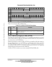
Bits 0 1 2 3 4 5 6 7 8 9 10 11 12 13 14 15
Field Ñ
Reset 0000_0000_0000_0000
R/W Read/write
Addr 0xF34
Bits 16 17 18 19 20 21 22 23 24 25 26 27 28 29 30 31
Field Ñ BC_REJ PROM MII_MODE DRT LOOP
Reset 0000_0000_0000_0000
R/W Read/write
Addr 0xF36
Figure 6-20. R_CNTRL Register
Fr
eescale S
emiconduct
or
, I
Freescale Semiconductor, Inc.
For More Information On This Product,
Go to: www.freescale.com
nc...