


DSP Bus Registers
There are two 32-bit registers in the DSP bus address space. The VXI
FPGA does not assert TA* when these registers are accessed.
200A DSP Command Register
200B
Boot Register
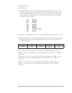
Note that these registers appear multiple times in the memory map, since
only the address lines A31-30, A17-13, A9-8, and A3-0 are used for decoding.
The A24 registers are defined as follows:
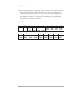
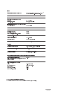
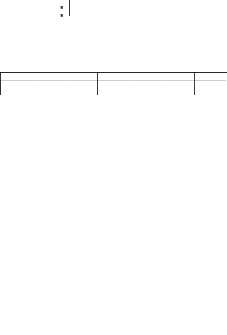
q Boot Register: This read/write register is used to configure the device after a
device reset. It has the following format:
Bit 31-16 15 14 13 12 11-0
Contents Unused
Spare ST Done Loaded Ready Model
Code
Spare: This read/write bit has no pre-defined function.
ST Done: This bit should be written to a one (1) when the DSP
successfully competes its self-test, within five seconds after SYSRESET* is
de-asserted. Its initial value is zero (0).
Loaded: This bit should be written to a one (1) when (or immediately
after) the DSP loads the model code, before competing its self-test. Its
initial value is zero (0).
Ready: This bit is written to a one (1) to indicate that the device is ready
for normal operation. Its initial value is zero (0).
Model Code: As soon as possible, and within 25 ms after coming out of
reset, when the DSP has valid code loaded, it should write the VXI model
code to these bits. Their initial value is 0x0200.
HP E1432A User's Guide
Register Definitions
A-15