


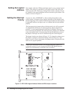

14 Installing and Configuring the HP E1459A
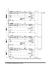
Watchdog Timer The HP E1459A provides a programmable timer facility which, in the event
of time-out, will generate a "system wide" reset to all other card-cage
modules. This timer may be disabled by the SCPI command
DIAG:SYSR:ENAB OFF.
Input Level
Selection
Each channel is capable of operation over an input range from 2.0 through
60.0 Vdc. Input voltages are grouped into voltage ranges which are selected
via a series of jumpers on the module. These jumpers are described in more
detail beginning on page 21.
Input Isolation Each channel is optically coupled and electrically isolated from all other
channels and current paths. Isolated channel inputs are polarized and require
that the user observe input signal polarity when connections are made.
Input Debounce
Processing
Each channel is debounced by a digital circuit specific to this function. Two
programmable clock sources establish reference parameters which
determine the debounce criteria for validating inputs. Channels are not
independently programmed for debounce period, but are instead grouped
together in blocks of 32 channels per clock source. Channels 00-31 (Ports 0
and 1) are collectively programmed via one clock source and channels 32-63
(Ports 2 and 3) are programmed via a second clock source.
Programmable
Debounce Parameters
Debounce circuits require that a channel input remain in a stable state for 4
to 4.5 periods of the programmable clock before a channel transition is
declared. The debounce clocks may be programmed for frequencies ranging
from 250 KHz down to 466 µHz. The 4 to 4.5 clock period requirements of
the debouncers translate into debounce periods which range from 16 µS
minimum to 9600 seconds (2.67 hours) maximum.
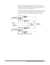
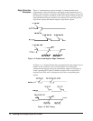
The debounce circuits can add considerable latency in the signal path and an
additional delay occurs within the Register FPGA. Normally the signals pass
though without significant delay. However, during a VXIbus transaction to
this port, the input signals are momentarily captured by a latch and are held
for the duration of the bus transaction plus 500 nS. This prevents data events
from being lost due to potential timing conflicts with VXIbus transactions.
The data signals are then synchronized with the system clock and
synchronously captured in either the data register, the positive edge event
register, or the negative edge event register. This can potentially add another
500 nS depending upon timing circumstances.
Thus the input data is delayed by the debounce circuits, possibly by the input
latches (equal to bus transaction time plus 500 nS), and a synchronizing
delay of 500 nS. The external clocks (front panel external trigger inputs) are
also delayed but by no more than 500 nS. Therefore, an external capture
clock concurrent with a data event will not capture the event unless
consideration is given for data latency.