USB-1616HS-2 User's Guide Functional Details
18
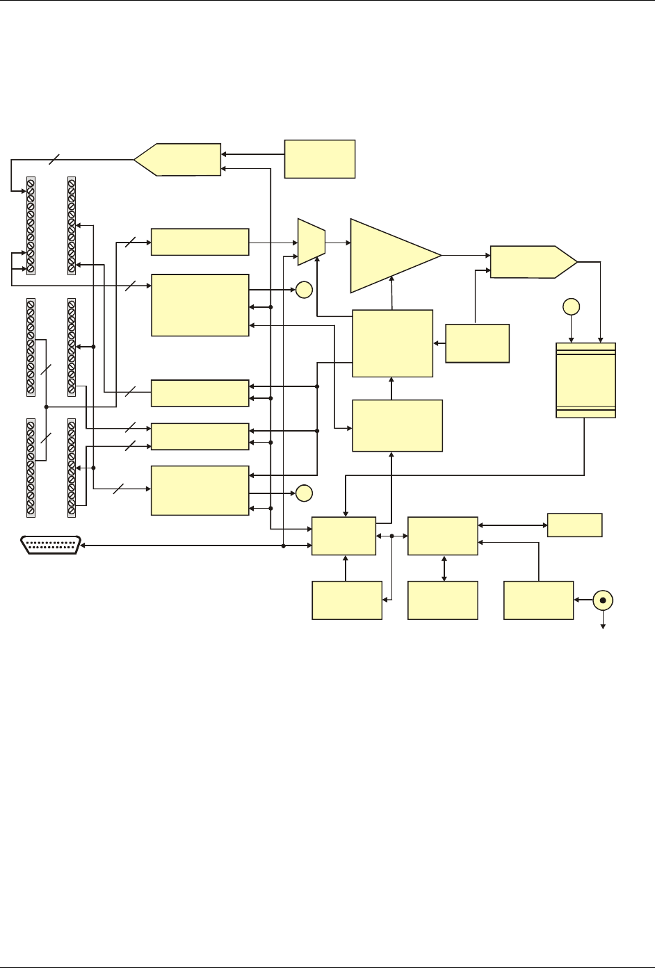
USB-1616HS-2 block diagram
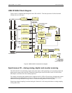
Figure 6 shows a simplified block diagram of the USB-1616HS-2. This board provides all of the functional
elements shown in the figure.
1 MHz
output clock
Analog channel
input protection
One TTL
trigger input
One analog
input pacer clock
Four 32-bit
counter inputs
Two 16-bit
Timer outputs
Three 8-bit
DIO ports
512-step
random access
channel/gain
sequencer
Programmable
sequencer
timebase
1 s to 6 hours
µ
System
controller
USB
controller
Configurable
EPROM
DC to DC
converter
USB port
16-bit
D/A converters
x1, x2,
x5, x10, x20
x50, x100
MUX
A
A
1 MSample
FIFO
Data Buffer
16-bit, 1 MHz
A/D converter
Configurable
PLD
8 diff/16 SE
analog inputs
2
Programmable gain
amplifier
8
8
16
2
2
2
2
24
A
1 MHz
input clock
Sequencer reset
DSUB25F
Expansion connector
External
power
Connect the optional
power supply
if the USB cannot
supply enough power.
Figure 6. USB-1616HS-2 functional block diagram
Synchronous I/O – mixing analog, digital, and counter scanning
The USB-1616HS-2 can read analog, digital, and counter inputs, while generating up to two analog outputs and
digital pattern outputs at the same time. Digital and counter inputs do not affect the overall A/D rate because
these inputs use no time slot in the scanning sequencer.
For example, one analog input channel can be scanned at the full 1 MHz A/D rate along with digital and counter
input channels. Each analog channel can have a different gain, and counter and digital channels do not need
additional scanning bandwidth as long as there is at least one analog channel in the scan group.
Digital input channel sampling is not done during the "dead time" of the scan period where no analog sampling
is being done either.


