


I
CONTENTS
CONTENTS
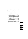
1. PLC FUNCTION 1
1.1 Function Block Diagram ...........................................................2
1.2 PLC Function Specifications....................................................3
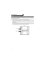
1.3 System Configuration ...............................................................4
1.4 Wiring of the Inverter and Personal Computer Using
GX Developer for RS-485 Communication..............................5
1.5 Prior to Sequence Program Creation ......................................6
1.5.1 Precautions for sequence program creation ................................................. 6
1.5.2 Usable main GX Developer functions ........................................................... 6
1.5.3 Sequence program execution key................................................................. 7
1.5.4 Sequence program write ............................................................................... 8
1.5.5 Setting list of built-in PLC function parameter ............................................... 9
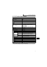
1.6 Device Map...............................................................................10
1.6.1 I/O device map ............................................................................................ 10
1.6.2 Internal relay (M) device map...................................................................... 12
1.6.3 Data register (D) device map ...................................................................... 12
1.6.4 Special relays.............................................................................................. 12
1.6.5 Special registers.......................................................................................... 14
1.7 Inverter Status Monitoring, Special Registers for Control ..20
1.7.1 Data that can be read at all times................................................................ 20
1.7.2 Data that are read by controlling (OFF to ON) the read command .............23
1.7.3 How to write data by controlling (OFF to ON) the write
command.................................................................................................... 25
1.7.4 Inverter operation status control.................................................................. 31
1.7.5 Inverter parameter access error (D9150)....................................................33
1.7.6 Inverter status (D9151)................................................................................ 33
1.8 Inverter Parameter Read/Write Method .................................34
1.8.1 Reading the inverter parameters................................................................. 34
1.8.2 Writing the inverter parameters...................................................................36
1.9 User Area Read/Write Method ................................................38
1.9.1 User parameter read/write method.............................................................. 38
1.10 Analog I/O function .................................................................39
1.10.1 Analog input ................................................................................................ 39
1.10.2 Analog output .............................................................................................. 39
1.11 Paluse train input function .....................................................40
1.12 PID control ...............................................................................41
1.13 Inverter Operation Lock Mode Setting ..................................43