


V
CCO
R/W
CE1
BA14–BA0
BD7–BD0
MSEL
CE2
V
CC
V
LI
PORT0
PORT1
PORT2
PORT3
GND
28
27
20
14
V
CC
WE
CS
A14–A0
D7–D0
GND
OE
32K x 8 SRAM
VCC
WE
CS
A14–A0
D7–D0
GND
OE
32K x 8
SRAM
28
27
20
14
V
CC
WE
CS
A14–A0
D7–D0
GND
OE
32K x 8
SRAM
22
22
+5V
14
2
12
10
74
13
54
+3V
+5V
52
DS5001FP/DS5002FP
USER’S GUIDE
050396 50/173
51
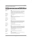
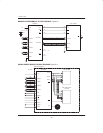
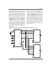
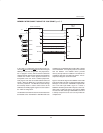
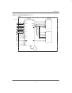
The DS5001FP has several memory options. It can be
connected to between one 8K byte SRAM and four
32K byte SRAMs. It will also support one 128K byte
SRAM. In most cases the DS5001FP is used for its
greater memory access so it will not be used with 8K
RAMs. In the Partitionable mode (see Section 4), the
DS5001FP can be connected to one or two SRAMs.
Figure 5–3 illustrates the connection of two 32K x 8
SRAMs. Each RAM has its own chip enable, with a com-
mon WE
generated by the DS5001FP R/W signal.
When using the DS5001FP with only one RAM, the se-
cond chip enable will simply remain unconnected. This
solution provides a total of 64K bytes of memory which
the user can partitions into program and data segments.
The Partition setting has no impact on the interconnect.
Using the Partition, the microcontroller determines which
memory blocks are program and write protects the ap-
propriate addresses.
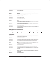
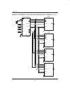
In the non–partitionable case, the DS5001FP can be
connected to three or four 32K x 8 SRAMs. The four
RAM case is shown in Figure 5–4. Each RAM has its
own chip enable. To use three RAMs, simply omit the
unused chip enable (CE2 or 4) as described in Section
4. In other ways, this hardware configuration is similar to
the Partitionable mode discussed above. While this
provides the full 128K bytes of memory, it requires more
space and cost than the version shown in Figure 5–5.
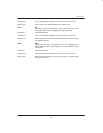
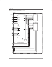
This uses the 128K byte SRAM. All program and data
memory is contained within the single chip. The DS5001
manages the addressing and decoding. Note the MSEL
signal is connected to ground to initiate this mode. The
PM bit and Range must still be configured by the user
during program loading.
MEMORY INTERCONNECT OF THE PARTITIONABLE DS5001/DS5002 Figure 5–3