


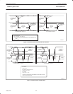
Philips Semiconductors Product specification
PDIUSBH12USB 2-port hub
1999 Jul 22
18
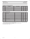
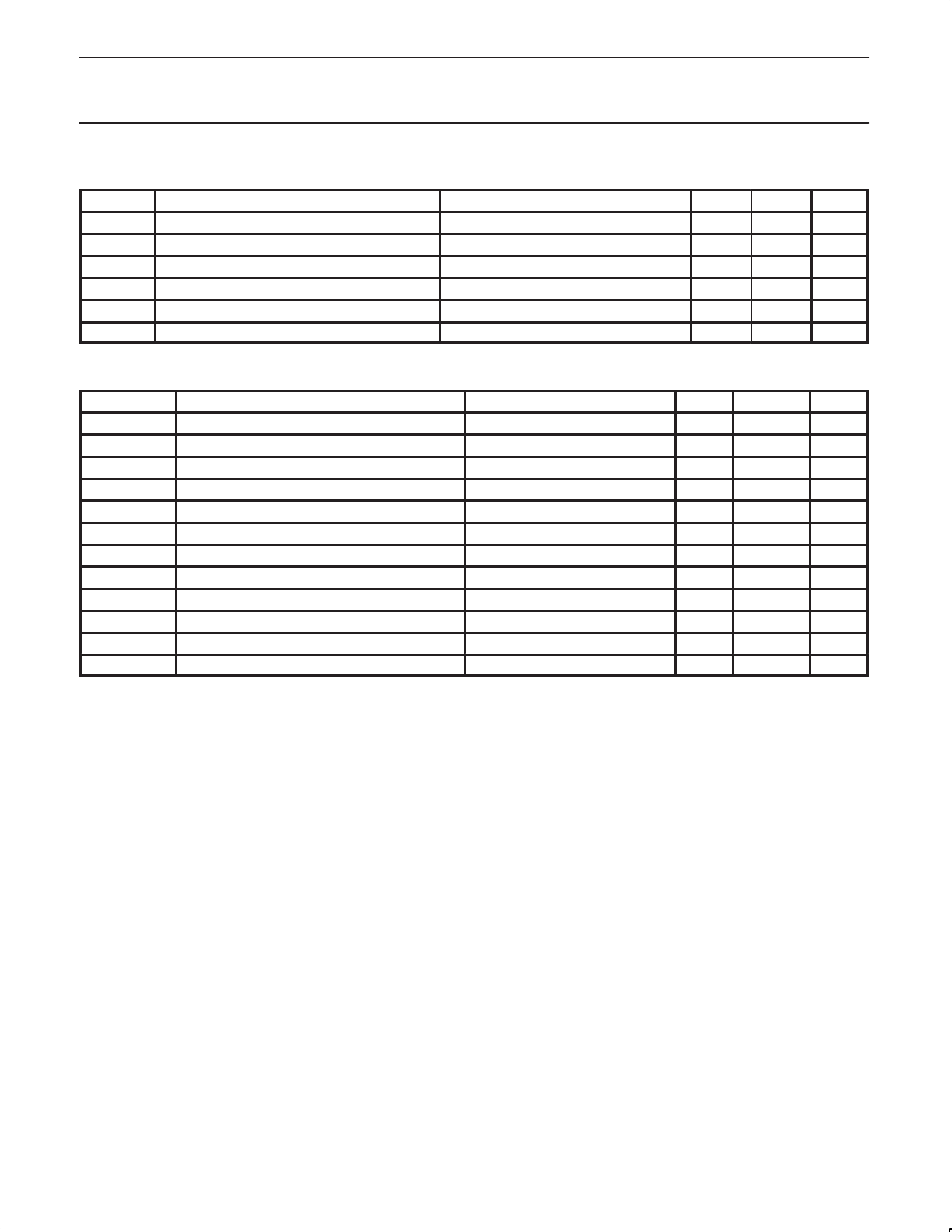
RECOMMENDED OPERATING CONDITIONS
SYMBOL PARAMETER TEST CONDITIONS MIN MAX UNIT
V
CC
DC supply voltage 3.0 3.6 V
V
I
DC input voltage range 0 5.5 V
V
I/O
DC input voltage range for I/O 0 5.5 V
V
AI/O
DC input voltage range for analog I/O 0 V
CC
V
V
O
DC output voltage range 0 V
CC
V
T
amb
Operating ambient temperature range in free air See DC and AC characteristics per device –40 85 °C
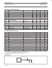
ABSOLUTE MAXIMUM RATINGS
1
SYMBOL
PARAMETER TEST CONDITIONS MIN MAX UNIT
V
CC
DC supply voltage –0.5 +4.6 V
I
IK
DC input diode current V
I
< 0 –50 mA
V
I
DC input voltage Note 2 –0.5 +5.5 V
V
I/O
DC input voltage range for I/O’s –0.5 V
CC
+ 0.5 V
I
OK
DC output diode current V
O
> V
CC
or V
O
< 0 ±50 mA
V
O
DC output voltage Note 2 –0.5 V
CC
+ 0.5 V
I
O
DC output sink or source current for other pins V
O
= 0 to V
CC
±15 mA
I
O
DC output sink or source current for D+/D– pins V
O
= 0 to V
CC
±50 mA
I
GND
, I
CC
DC V
CC
or GND current ±100 mA
V
ESD
Electrostatic discharge voltage I
IL
< 1 µA
3
— ±4000
4
V
T
STG
Storage temperature range –60 +150 °C
P
TOT
Power dissipation per package
NOTES:
1. Stresses beyond those listed may cause damage to the device. These are stress ratings only and functional operation of the device at these
or any other conditions beyond those listed in the RECOMMENDED OPERATING CONDITIONS table is not implied. Exposure to absolute
maximum rated conditions for extended periods may affect device reliability.
2. The input and output voltage ratings may be exceeded if the input and output current ratings are observed.
3. Values are given for device only: in-circuit V
ESD(MAX)
= ±8000 V.
4. For open-drain pins V
ESD(MAX)
= ±2000 V.