


Philips Semiconductors Product specification
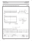
PDIUSBH12USB 2-port hub
1999 Jul 22
27
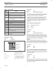
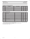
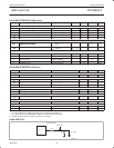
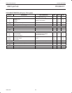
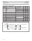
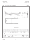
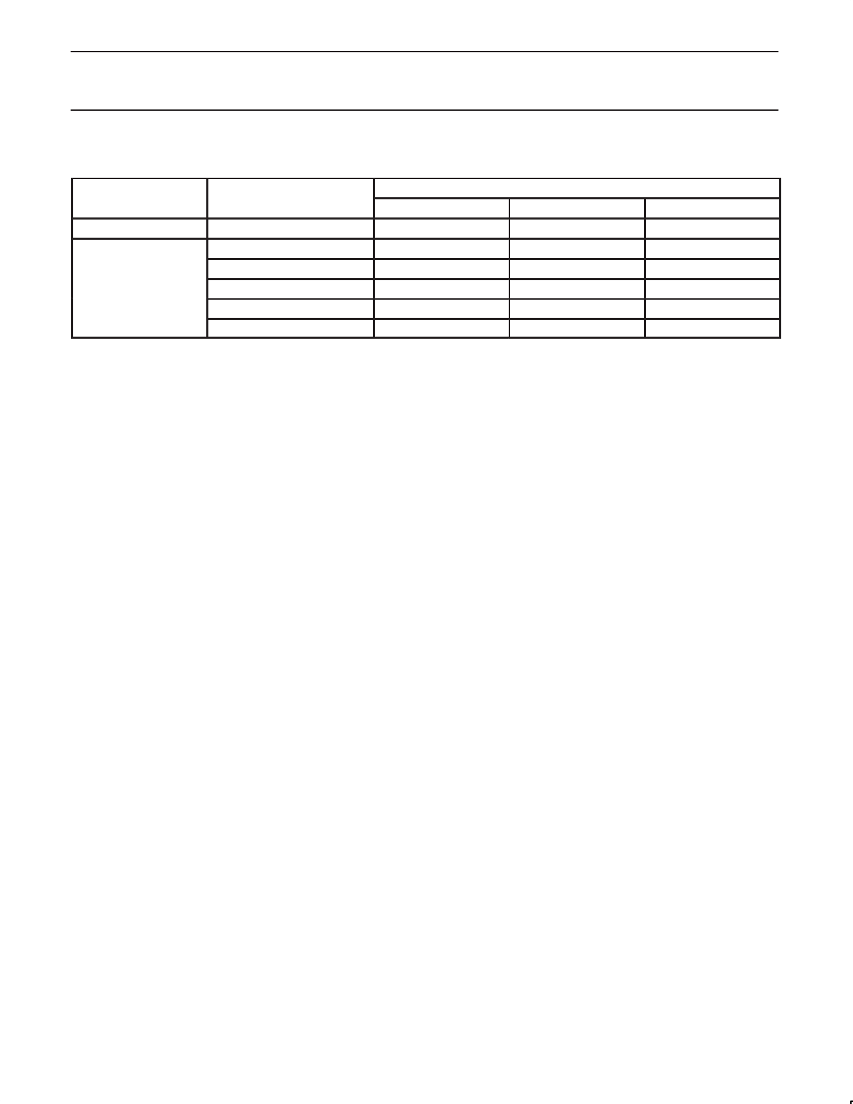
SUITABILITY OF IC PACKAGES FOR WAVE, REFLOW AND DIPPING SOLDERING METHODS
Mo nting
Package
Soldering Method
Mo
u
nting
Package
Wave Reflow
1
Dipping
Through-hole mount DBS, DIP, HDIP, SDIP, SIL suitable
2
– suitable
BGA, SQFP, not suitable suitable –
HLQFP, HSQFP, HSOP, SMS not suitable
3
suitable –
Surface mount PLCC, SO, SOJ suitable suitable –
LQFP, QFP, TQFP not recommended
4,
5
suitable –
SSOP, TSSOP, VSO not recommended
6
suitable –
NOTES:
1. All surface mount (SMD) packages are moisture sensitive. Depending upon the moisture content, the maximum temperature (with respect to
time) and body size of the package, there is a risk that internal or external package cracks may occur due to vaporization of the moisture in
them (the so-called “popcorn” effect). For details, refer to the Drypack information in the
“Data Handbook IC26; Integrated Circuit Packages;
Section: Packing Methods”.
2. For SDIP packages, the longitudinal axis must be parallel to the transport direction of the printed-circuit board.
3. These packages are not suitable for wave soldering as a solder joint between the printed-circuit board and heatsink (at bottom version)
cannot be achieved, and as solder may stick to the heatsink (on top version).
4. If wave soldering is considered, then the package must be placed at a 45° angle to the solder wave direction. The package footprint must
incorporate solder thieves downstream and at the side corners.
5. Wave soldering is only suitable for LQFP, QFP, and TQFP packages with a pitch (e) equal to or larger than 0.8 mm; it is definitely not
suitable for packages with a pitch (e) equal to or smaller than 0.65 mm.
6. Wave soldering is only suitable for SSOP and TSSOP packages with a pith (e) equal to or larger than 0.65 mm; it is definitely not suitable for
packages with a pitch (e) equal to or smaller than 0.5 mm.