


( 57 / 80 )
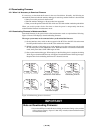
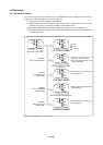
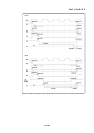
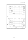
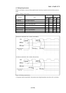
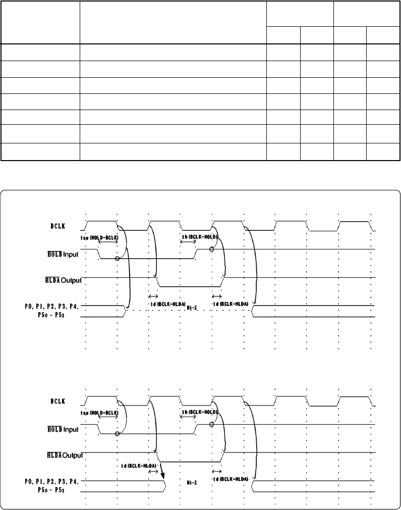
Figure 5.3 Timing requirements
* Compared with an actual MCU, this product enters high-impedance state after a 0.5 cycle delay.
Vcc1 = Vcc2 = 5 V
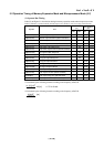
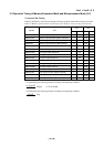
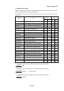
(3) Timing Requirements
Tables 5.4 and Figure 5.3 list the timing requirements.
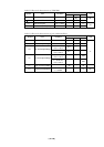
Table 5.4 Timing requirements
Symbol Item
Actual MCU
[ns]
This product
[ns]
Min. Max.Min. Max.
tsu(DB-RD)
tsu(RDY-BCLK)
tsu(HOLD-BCLK)
th(RD-DB)
th(BCLK-RDY)
th(BCLK-HOLD)
td(BCLK-HLDA)
Data input setup time
RDY* input setup time
HOLD* input setup time
Data input hold time
RDY* input hold time
HOLD* input hold time
HLDA* output delay time
40
30
40
0
0
0
40
55
45
55
See left
See left
See left
Common to "with wait" and "no-wait" (this product)
Common to "with wait" and "no-wait" (actual MCU)
See left