


( 58 / 80 )
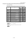
Vcc1 = Vcc2 = 3 V
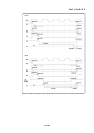
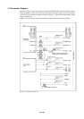
5.3 Operation Timing of Memory Expansion Mode and Microprocessor Mode (3 V)
(1) Separate Bus Timing
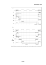
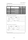
Table 5.5 and Figure 5.4 show the bus timing in memory expansion mode and microprocessor mode.
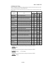
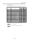
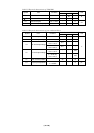
Table 5.5 Memory expansion mode and microprocessor mode (3-wait, accessing external area)
-40 [ns] n: "3" for 3-wait
(
n
- 0.5)x10
9
f (BCLK)
[ns]
0.5x10
9
f (BCLK)
Symbol
Item
Actual MCU
[ns]
This product
[ns]
Min. Max.
td(BCLK-AD)
th(BCLK-AD)
th(RD-AD)
th(WR-AD)
td(BCLK-CS)
th(BCLK-CS)
td(BCLK-ALE)
th(BCLK-ALE)
td(BCLK-RD)
th(BCLK-RD)
td(BCLK-WR)
th(BCLK-WR)
td(BCLK-DB)
th(BCLK-DB)
td(DB-WR)
th(WR-DB)
Address output delay time
Address output hold time (BCLK standard)
Address output hold time (RD standard)
Address output hold time (WR standard)
Chip-select output delay time
Chip-select output hold time (BCLK standard)
ALE signal output delay time
ALE signal output hold time
RD signal output delay time
RD signal output hold time
WR signal output delay time
WR signal output hold time
Data output delay time (BCLK standard)
Data output hold time (BCLK standard)
Data output delay time (WR standard)
Data output hold time (WR standard)
4
0
(*2)
4
-4
0
0
4
(*1)
(*2)
Max.
30
30
30
30
30
40
Min.
*1 Calculated by the following formula according to the frequency of BCLK.
*2 Calculated by the following formula according to the frequency of BCLK.
See left
See left
See left
See left
See left
See left
See left
See left
See left
See left
See left
See left
See left
See left
See left
See left