CY7C63310, CY7C638xx
Document 38-08035 Rev. *K Page 37 of 83
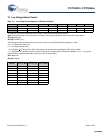
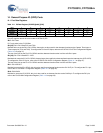
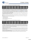
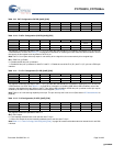
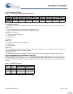
Table 14-7. P0.2/INT0–P0.4/INT2 Configuration (P02CR–P04CR) [0x07–0x09] [R/W]
Bit # 7 6 5 4 3 2 1 0
Field Reserved Int Act Low TTL Thresh Reserved Open Drain Pull up Enable Output Enable
Read/Write – – R/W R/W –R/WR/W R/W
Default 0 0 0 0 000 0
These registers control the operation of pins P0.2–P0.4 respectively. The pins are shared between the P0.2–P0.4 GPIOs and
the INT0–INT2. These registers exist in all enCoRe II parts. The INT0–INT2 interrupts are different from all the other GPIO
interrupts. These pins are connected directly to the interrupt controller to provide three edge sensitive interrupts with independent
interrupt vectors. These interrupts occur on a rising edge when Int act Low is clear and on a falling edge when Int act Low is set.
The pins are enabled as interrupt sources in the interrupt controller registers (Table 17-8 on page 55 and Table 17-6 on page 53).
To use these pins as interrupt inputs, configure them as inputs by clearing the corresponding Output Enable. If the INT0–INT2
pins are configured as outputs with interrupts enabled, firmware can generate an interrupt by writing the appropriate value to the
P0.2, P0.3 and P0.4 data bits in the P0 Data Register.
Regardless of whether the pins are used as Interrupt or GPIO pins the Int Enable, Int act Low, TTL Threshold, Open Drain, and
Pull Up Enable bits control the behavior of the pin.
The P0.2/INT0–P0.4/INT2 pins are individually configured with the P02CR (0x07), P03CR (0x08), and P04CR (0x09) respec-
tively.
Note Changing the state of the Int Act Low bit can cause an unintentional interrupt to be generated. When configuring these
interrupt sources, it is best to follow the following procedure:
1. Disable interrupt source
2. Configure interrupt source
3. Clear any pending interrupts from the source
4. Enable interrupt source
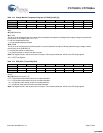
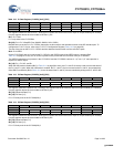
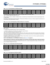
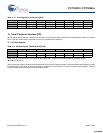
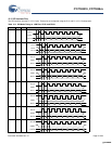
Table 14-8. P0.5/TIO0 – P0.6/TIO1 Configuration (P05CR–P06CR) [0x0A–0x0B] [R/W]
Bit # 7 6 5 4 3 2 1 0
Field TIO Output Int Enable Int Act Low TTL Thresh Reserved Open Drain Pull up Enable Output Enable
Read/Write – R/W R/W R/W –R/WR/W R/W
Default 0 0 0 0 000 0
These registers control the operation of pins P0.5 through P0.6, respectively. These registers exist in all enCoRe II parts.
P0.5 and P0.6 are shared with TIO0 and TIO1, respectively. To use these pins as Capture Timer inputs, configure them as inputs
by clearing the corresponding Output Enable. To use TIO0 and TIO1 as Timer outputs, set the TIOx Output and Output Enable
bits. If these pins are configured as outputs and the TIO Output bit is clear, firmware can control the TIO0 and TIO1 inputs by
writing the value to the P0.5 and P0.6 data bits in the P0 Data Register.
Regardless of whether either pin is used as a TIO or GPIO pin the Int Enable, Int act Low, TTL Threshold, Open Drain, and Pull
Up Enable control the behavior of the pin.
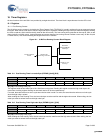
TIO0(P0.5) when enabled outputs a positive pulse from the Free Running Timer. This is the same signal that is used internally
to generate the 1024 μs timer interrupt. This signal is not gated by the interrupt enable state. The pulse is active for one cycle
of the capture timer clock.
TIO1(P0.6) when enabled outputs a positive pulse from the programmable interval timer. This is the same signal that is used
internally to generate the programmable timer interval interrupt. This signal is not gated by the interrupt enable state. The pulse
is active for one cycle of the interval timer clock.
The P0.5/TIO0 and P0.6/TIO1 pins are individually configured with the P05CR (0x0A) and P06CR (0x0B), respectively.
[+] Feedback [+] Feedback


