CY7C63310, CY7C638xx
Document 38-08035 Rev. *K Page 69 of 83
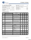
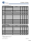
V
DI
Differential Input Sensitivity 0.2 V
V
CM
Differential Input Common Mode
Range
0.8 2.5 V
V
SE
Single Ended Receiver Threshold 0.8 2 V
C
IN
Transceiver Capacitance 20 pF
I
IO
Hi-Z State Data Line Leakage 0V < V
IN
< 3.3V –10 10 μA
PS/2 Interface
V
OLP
Static Output Low SDATA or SCLK pins 0.4 V
R
PS2
Internal PS/2 Pull up Resistance SDATA, SCLK pins, PS/2 Enabled 3 7 KΩ
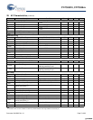
General Purpose IO Interface
R
UP
Pull Up Resistance 4 12 KΩ
V
ICR
Input Threshold Voltage Low, CMOS
mode
[8]
Low to High edge 40% 65% V
CC
V
ICF
Input Threshold Voltage Low, CMOS
mode
[8]
High to Low edge 30% 55% V
CC
V
HC
Input Hysteresis Voltage, CMOS
Mode
[8]
High to low edge 3% 10% V
CC
V
ILTTL
Input Low Voltage, TTL Mode
[9]
IO pin Supply = 4.0–5.5V 0.8 V
V
IHTTL
Input High Voltage, TTL Mode
[9]
IO pin Supply = 4.0–5.5V 2.0 V
V
OL1
Output Low Voltage, High Drive
[7]
I
OL1
= 50 mA 0.8 V
V
OL2
Output Low Voltage, High Drive
[7]
I
OL1
= 25 mA 0.4 V
V
OL3
Output Low Voltage, Low Drive
[8]
I
OL2
= 8 mA 0.4 V
V
OH
Output High Voltage
[8]
I
OH
= 2 mA V
CC
– 0.5 V
C
LOAD
Maximum Load Capacitance
[9]
50 pF
27. DC Characteristics
(continued)
Parameter
Description
Conditions Min Typical Max Unit
General
28. AC Characteristics
Parameter Description Conditions Min Typical Max Unit
Clock
T
ECLKDC
External Clock Duty Cycle 45 55 %
T
ECLK1
External Clock Frequency External clock is the source of the
CPUCLK
0.187 24 MHz
T
ECLK2
External Clock Frequency External clock is not the source of the
CPUCLK
024MHz
F
IMO1
Internal Main Oscillator Frequency No USB present 22.8 25.2 MHz
F
IMO2
Internal Main Oscillator Frequency With USB present 23.64 24.3 MHz
F
ILO1
Internal Low Power Oscillator Normal mode 29.44 37.12 kHz
F
ILO2
Internal Low Power Oscillator Low power mode 35.84 47.36 kHz
3.3V Regulator
V
ORIP
Output Ripple Voltage 10 Hz to 100 MHz at CLOAD = 1 μF 200 mV
p-p
Notes
7. Available only in CY7C638xx P1.3, P1.4, P1.5, P1.6, P1.7.
8. Except for pins P1.0 and P1.1 in the GPIO mode.
9. Except for pins P1.0 and P1.1.
[+] Feedback [+] Feedback


