CY7C63310, CY7C638xx
Document 38-08035 Rev. *K Page 56 of 83
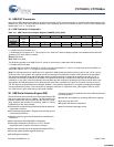
18. Regulator Output
18.1 VREG Control
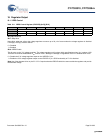
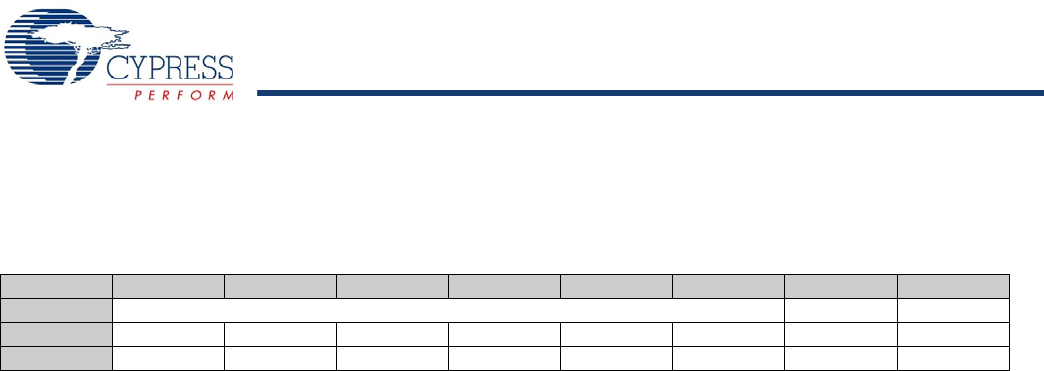
Table 18-1. VREG Control Register (VREGCR) [0x73] [R/W]
Bit # 7 6 5 4 3 2 1 0
Field Reserved Keep Alive VREG Enable
Read/Write – – – – – – R/W R/W
Default 0 0 0 0 000 0
Bit [7:2]: Reserved
Bit 1: Keep Alive
Keep Alive, when set, allows the voltage regulator to source up to 20 µA of current when the voltage regulator is disabled.
P12CR[0],P12CR[7] must be cleared.
0 = Disabled
1 = Enabled
Bit 0: VREG Enable
This bit turns on the 3.3V voltage regulator. The voltage regulator only functions within specifications when V
CC
is above 4.35V.
This block must not be enabled when V
CC
is below 4.35V—although no damage or irregularities occur if it is enabled below 4.35V.
0 = Disable the 3.3V voltage regulator output on the VREG/P1.2 pin.
1 = Enable the 3.3V voltage regulator output on the VREG/P1.2 pin. GPIO functionality of P1.2 is disabled.
Note Use of the alternate drive on pins P1.3–P1.6 requires that the VREG Enable bit be set to enable the regulator and provide
the alternate voltage.
[+] Feedback [+] Feedback


