CY7C63310, CY7C638xx
Document 38-08035 Rev. *K Page 41 of 83
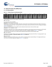
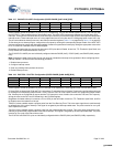
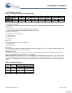
15.2 SPI Configure Register
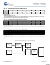
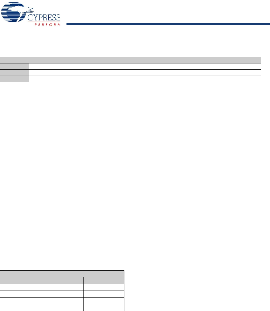
Table 15-2. SPI Configure Register (SPICR) [0x3D] [R/W]
Bit # 7 6 5 4 3 2 1 0
Field Swap LSB First Comm Mode CPOL CPHA SCLK Select
Read/Write R/W R/W R/W R/W R/W R/W R/W R/W
Default 0 0 0 0 000 0
Bit 7: Swap
0 = Swap function disabled.
1 = The SPI block swaps its use of SMOSI and SMISO. This is useful in implementing single wire communications similar to SPI.
Bit 6: LSB First
0 = The SPI transmits and receives the MSB (Most Significant Bit) first.
1 = The SPI transmits and receives the LSB (Least Significant Bit) first.
Bit [5:4]: Comm Mode [1:0]
0 0: All SPI communication disabled.
0 1: SPI master mode
1 0: SPI slave mode
1 1: Reserved
Bit 3: CPOL
This bit controls the SPI clock (SCLK) idle polarity.
0 = SCLK idles low
1 = SCLK idles high
Bit 2: CPHA
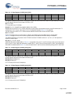
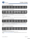
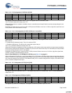
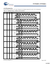
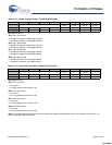
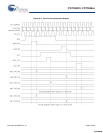
The Clock Phase bit controls the phase of the clock on which data is sampled. Table 15-4 on page 42 shows the timing for the
various combinations of LSB First, CPOL, and CPHA.
Bit [1:0]: SCLK Select
This field selects the speed of the master SCLK. When in master mode, SCLK is generated by dividing the base CPUCLK.
Note for Comm Modes 01b or 10b (SPI Master or SPI Slave)
When configured for SPI, (SPI Use = 1 Table 14-14 on page 39), the input/output direction of pins P1.3, P1.5, and P1.6 is set
automatically by the SPI logic. However, pin P1.4's input/output direction is NOT automatically set; it must be explicitly set by
firmware. For SPI Master mode, pin P1.4 must be configured as an output; for SPI Slave mode, pin P1.4 must be configured as
an input.
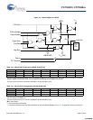
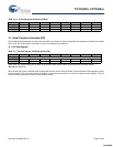
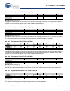
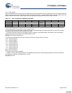
Table 15-3. SPI SCLK Frequency
SCLK
Select
CPUCLK
Divisor
SCLK Frequency when CPUCLK =
12 MHz 24 MHz
00 6 2 MHz 4 MHz
01 12 1 MHz 2 MHz
10 48 250 kHz 500 kHz
11 96 125 kHz 250 kHz
[+] Feedback [+] Feedback


