CY7C63310, CY7C638xx
Document 38-08035 Rev. *K Page 40 of 83
15. Serial Peripheral Interface (SPI)
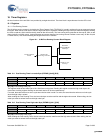
The SPI Master/Slave Interface core logic runs on the SPI clock domain, so that its functionality is independent of system clock speed.
SPI is a four pin serial interface comprised of a clock, an enable and two data pins.
15.1 SPI Data Register
When an interrupt occurs to indicate to the firmware that a byte of receive data is available, or the transmitter holding register is empty,
the firmware has 7 SPI clocks to manage the buffers: to empty the receiver buffer or to refill the transmit holding register. Failure to
meet this timing requirement results in incorrect data transfer.
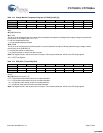
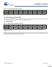
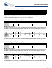
Table 14-17. P3 Configuration (P3CR) [0x16] [R/W]
Bit # 7 6 5 4 3 2 1 0
Field Reserved Int Enable Int Act Low TTL Thresh Reserved Open Drain Pull up Enable Output Enable
Read/Write – R/W R/W R/W - R/W R/W R/W
Default 0 0 0 0 0 0 1 0
This register exists in CY7C638(2/3)3. This register controls the operation of pins P3.0–P3.1.
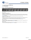
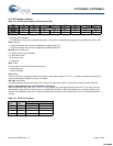
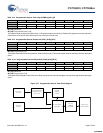
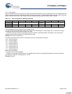
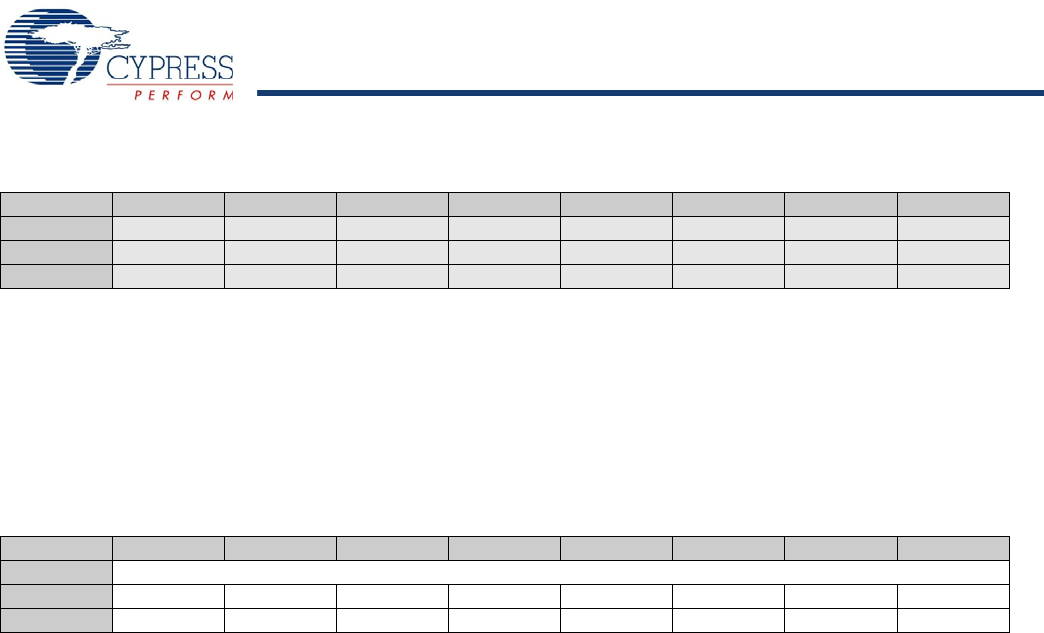
Table 15-1. SPI Data Register (SPIDATA) [0x3C] [R/W]
Bit # 7 6 5 4 3 2 1 0
Field SPIData[7:0]
Read/Write R/W R/W R/W R/W R/W R/W R/W R/W
Default 0 0 0 0 000 0
When read, this register returns the contents of the receive buffer. When written, it loads the transmit holding register.
Bit [7:0]: SPI Data [7:0]
[+] Feedback [+] Feedback


