


4-2 361834-002 Technical Reference Guide
System Support
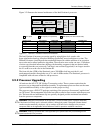
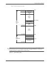
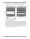
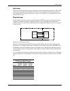
Figure 4-1. PCI Bus Devices and Functions
4.2.1 PCI 2.3 Bus Operation
The PCI 2.3 bus consists of a 32-bit path (AD31-00 lines) that uses a multiplexed scheme for
handling both address and data transfers. A bus transaction consists of an address cycle and one
or more data cycles, with each cycle requiring a clock (PCICLK) cycle. High performance is
realized during burst modes in which a transaction with contiguous memory locations requires
that only one address cycle be conducted and subsequent data cycles are completed using
auto-incremented addressing. Four types of address cycles can take place on the PCI bus; I/O,
memory, configuration, and special. Address decoding is distributed (left up to each device on
the PCI bus).
I/O and Memory Cycles
For I/O and memory cycles, a standard 32-bit address decode (AD31..0) for byte-level
addressing is handled by the appropriate PCI device. For memory addressing, PCI devices
decode the AD31..2 lines for dword-level addressing and check the AD1,0 lines for burst
(linear-incrementing) mode. In burst mode, subsequent data phases are conducted a dword at a
time with addressing assumed to increment accordingly (four bytes at a time).
82915G/GV [1]
82801 ICH6
Host-DMI Bridge
Memory
Cntlr
Function
PCI Express x16 graphics slot [2]
PCI Bus 0
IDE
Cntlr
Function
SATA
Cntlr
Function
USB I/F
Cntlr
Function
LPC
Bridge
Function
AC97
Cntlr
Function
DMI
PCI Express x1 slot [1]
PCI 2.3 slot(s)
Integrated
Graphics
Controller
PCI 2.3
Bridge
Function
GMCH
PCI Bus 1
Host-PCI Exp.
Bridge
NIC
Cntlr
PCI Exp.
Port 1
Function
DMI Link
RGB Monitor
[1] USDT form factor; 82915GV; SFF, ST, MT, and CMT form factors, 82915G
Notes:
PCI Exp.
Port 2
Function
[2] SFF. ST, MT, and CMT form factors only.