


Hardware Overview 39
• 32 KB four-way set-associative instruction cache
• 32 KB four-way set-associative data cache
• 64-bit memory interface with 32-bit addressing
• Virtual memory support for up to 4 petabytes (2
52
)
• Real memory support for up to 4 gigabytes
• ˜5.1 million transistors
• Nap power management mode
• JTAG bus (IEEE 1149.1) for RAS
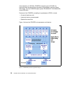
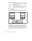
2.5 SMP Hardware Characteristics
Sharing resources is probably the main technical issue in the design of a
symmetric multiprocessor (SMP) system. To support symmetric
multiprocessing, specific techniques must be provided at the hardware level
and the software level. This section introduces the memory hierarchy concept
and some of the techniques used to solve resource-sharing and contention
issues.
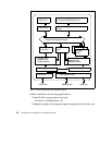
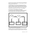
2.5.1 Memory Hierarchy
In order to improve the hardware performance of a system (uniprocessor
(UP) or mulitprocessor (MP), different levels of memory are used. These
different levels of memory can be ordered according to their access time and
capacity.
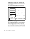
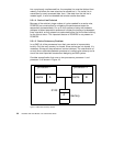
If you look at the different types of memory available on a typical system, you
will find the CPU registers at one end. They are fast but small, and have a
high cost per bit. At the other end, you will find the disks, which are slow but
have a very low cost per bit, allowing for high disk storage capacity.
In most UP or SMP implementations, a first level of cache (L1) lies between
these two ends. L1 cache is a fast form of memory with a small capacity. The
number of CPU cycles that are needed for the processor to load data from L1
depends on the L1 implementation, In the PowerPC implementation, L1 is on
the CPU chip itself, so it takes only one cycle to load data from L1. When the
L1 cache is outside the processor chip, several cycles are required to load
data from L1. A typical L1 capacity is around 32 to 64 KB.
You might also find a second level of cache (L2), which is another form of
high-speed memory. It takes about two to ten cycles to load data from L2.